6 footprint, 1 components location, Footprint – Sundance SMT381 2007 User Manual
Page 18: Components location, Figure 12: connector location on smt381
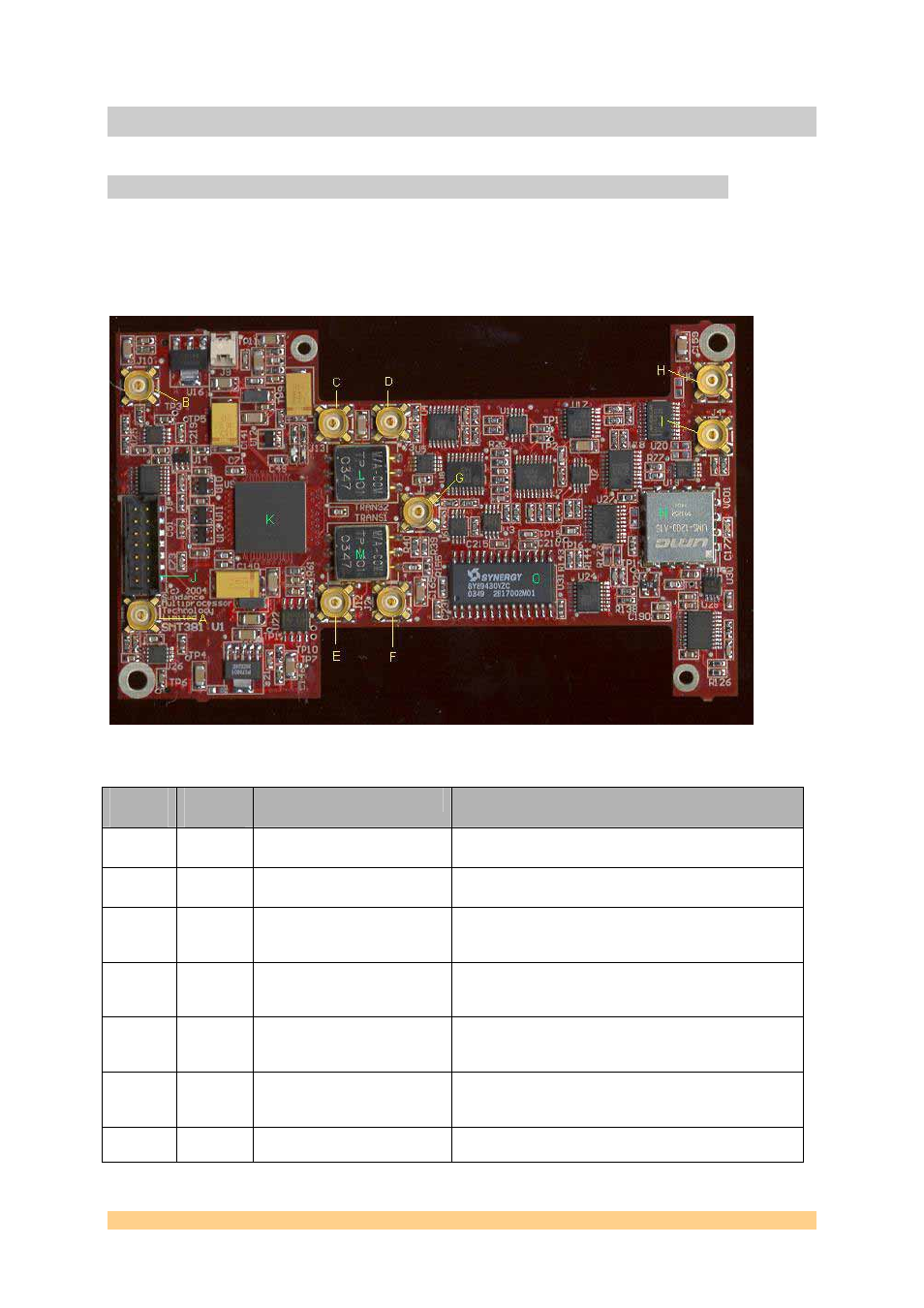
6 Footprint
6.1 Components location
The following diagram indicates the location of all the important connectors and
components on the SMT381 (Rev 1) PCB.
Figure 12: Connector Location on SMT381
Diagram
Ref
Pcb
RefDes
Description
Notes
A
J11
External Trigger B Channel
LVPECL Signal. Positive on inside of connector. Negative
on outside of connector.
B
J10
External Trigger A Channel
LVPECL Signal. Positive on inside of connector. Negative
on outside of connector.
C
J13
DAC Output B Channel (neg)
Analog Signal. Signal on inside of connector. GND on
outside of connector. For DC Coupling only (differential
signal, split over both connectors).
D
J3
DAC Output B Channel (pos)
Analog Signal. Signal on inside of connector. GND on
outside of connector. For AC Coupling (single ended), and
pos side of DC coupling (differential)
E
J12
DAC Output A Channel (neg)
Analog Signal. Signal on inside of connector. GND on
outside of connector. For DC Coupling only (differential
signal, split over both connectors).
F
J2
DAC Output A Channel (pos)
Analog Signal. Signal on inside of connector. GND on
outside of connector. For AC Coupling (single ended), and
pos side of DC coupling (differential).
G
J1
DAC Test Clock Output
LVPECL output test clock. Copy of clock going to DAC.
Postive on inside of connector, negative on outside of
User Manual SMT381
Last Edited: 12/06/2007 10:43:00