Figure 15: pinout jtag header – jp1, Figure 16: pinout jtag header – jp1 – Sundance SMT368 User Manual
Page 22
Note: An adapter is necessary to connect the JTAG Header JP1 to the Xilinx
Parallel cable IV. Please ask your Sundance technical or sales person for
ordering information.
All devices from the Block_1 (FPGA, CPLD, PROM) are chained, and they are accessible via
this JTAG header.
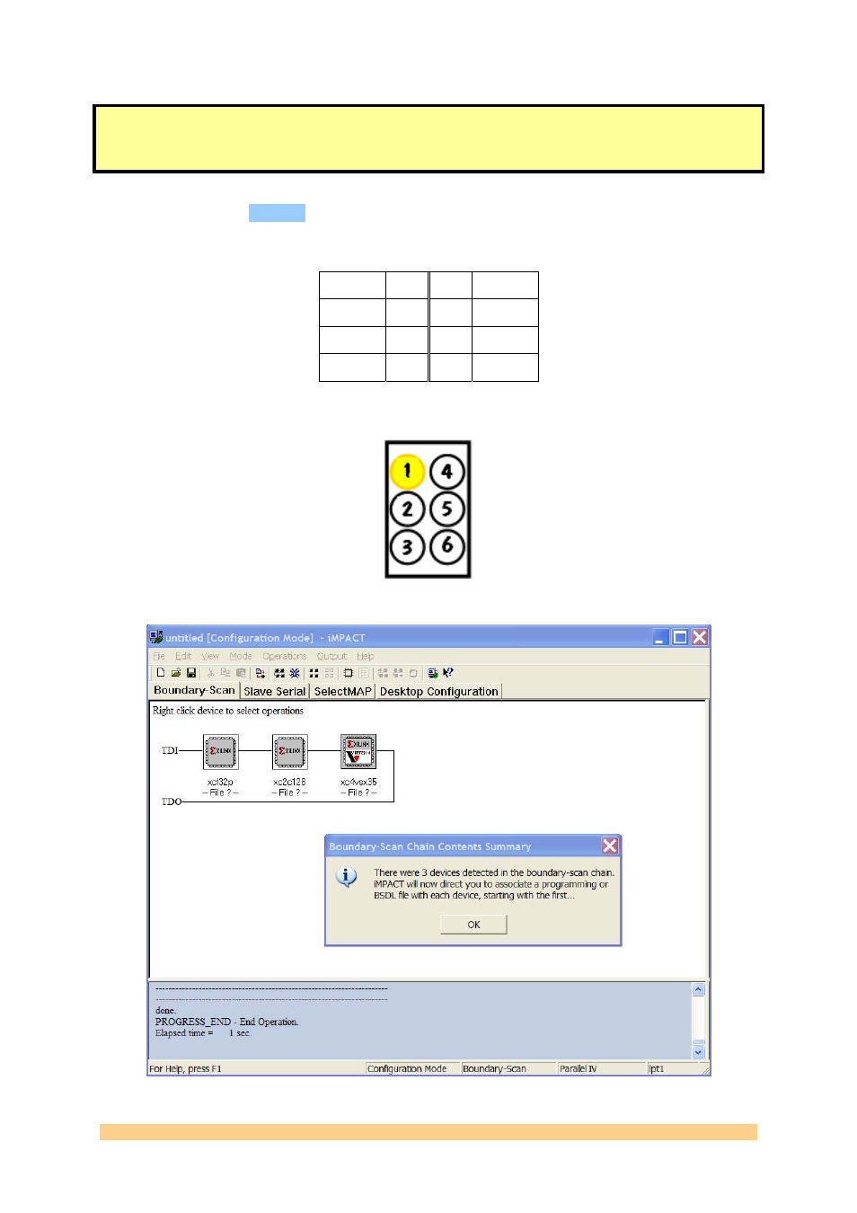
Signal Pin Pin Signal
VCC 1 4 TMS
GND 2 5 TDI
TCK 3 6 TDO
Figure 15: Pinout JTAG header – JP1
Figure 16: Pinout JTAG header – JP1
User Manual SMT368
Page 22 of 24
Last Edited: 31/12/2008 13:53:00
See also other documents in the category Sundance Equipment:
- SMT107 (16 pages)
- SMT6035 v.2.2 (39 pages)
- SMT6012 v.4.6 (22 pages)
- FC100 (12 pages)
- FC108 v.1.1 (10 pages)
- SMT6065 v.4.0 (45 pages)
- FFT v.2.1 (19 pages)
- SMT111 (18 pages)
- SMT118LT (10 pages)
- SMT118 (20 pages)
- SMT123-SHB (13 pages)
- SMT128 (15 pages)
- SMT145 (18 pages)
- SMT148 (35 pages)
- SMT130 v.1.0 (46 pages)
- SMT148FX (48 pages)
- SMT310Q (55 pages)
- PARS (70 pages)
- SMT166-FMC (52 pages)
- SMT166 (44 pages)
- SMT300Q v.1.6 (61 pages)
- SMT310 v.1.6 (50 pages)
- SMT317 (24 pages)
- SMT326v2 (24 pages)
- SMT338 (19 pages)
- SMT349 (32 pages)
- SMT339 v.1.3 (27 pages)
- SMT338-VP (22 pages)
- SMT358 (25 pages)
- SMT351T (37 pages)
- SMT351 (25 pages)
- SMT350 (45 pages)
- SMT362 (30 pages)
- SMT365G (23 pages)
- SMT364 (37 pages)
- SMT373 (15 pages)
- SMT370v3 (46 pages)
- SMT377 (22 pages)
- SMT381 2007 (31 pages)
- SMT381-VP (81 pages)
- SMT387 (42 pages)
- SMT391 (18 pages)
- SMT384 (47 pages)
- SMT390-VP (55 pages)