12 leds, 13 i/os, 2 module description – Sundance SMT368 User Manual
Page 13: 1 fpga configuration, Leds, I/os, Module description, Fpga configuration, Figure 7: schematics of the external clock i/o, Table 2: leds connections
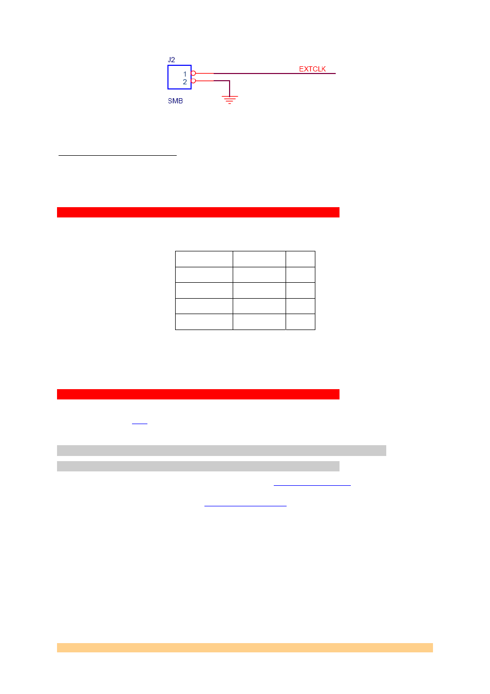
Figure 7: Schematics of the External Clock I/O
Constraints file signal names:
BOARDCLK
On-board oscillator input to the FPGA (pin AF10)
EXT_CLK
External Clock input to the FPGA (pin AF11: IO_L4P_GC_LC_4)
4.1.12 LEDs
There are six LEDs on the SMT368:
• Four LEDs are connected to the FPGA and they are available as I/Os:
UCF name FPGA pin LED
LED0 H3
D3
LED1 H4
D4
LED2 H5
D5
LED3 H6
D6
Table 2: LEDs connections
• One LED (D1) is connected to the DONE pin of the FPGA to show that the FPGA is
configured.
• One LED (D2) is connected to a I/O (pin 99) of the CPLD.
4.1.13 I/Os
There are four TTL I/Os that are directly connected to the FPGA. They are connected to the
pin-socket header
4.2 Module Description
4.2.1 FPGA Configuration
The general FPGA configuration is described in
er to the
chapter Configuring the FPGA section FPGA type TIM. To illustrate the FPGA
configuration, please refer to the
from the Knowledge Base in the
Support forum.
Different schemes are available to provide a maximum flexibility in systems where the
SMT368 is involved. The FPGA can be configured in three different ways:
• Using the ComPort_3 (CP_3) or ComPort_0 (CP_0) to provide the bitstream,
• Using the on-board JTAG header (JP1) and the JTAG programming tools,
• Using the on-board Xilinx PROM.
User Manual SMT368
Page 13 of 24
Last Edited: 31/12/2008 13:53:00