9 tim connectors, 10 dip switches, 11 clocking scheme – Sundance SMT368 User Manual
Page 12: Tim connectors, Dip switches, Clocking scheme, Figure 6: comport constraints file signal names, Table 1: external clock specification
4.1.9 TIM Connectors
TIM connectors provide 4 ComPorts to the FPGA: ComPort_0, 1, 3 and 4.
They allow interfacing to Sundance modules or to a host by implementing a ComPort
interface in the FPGA.
The ComPort interface is available in the
.
The FPGA I/O banks hosting the ComPort signals are powered using Vcco=3.3V.
The TIM connectors also provide the power and ground rails, reset and various control
signals.
The references and the specification documents for these connectors are available from our
.
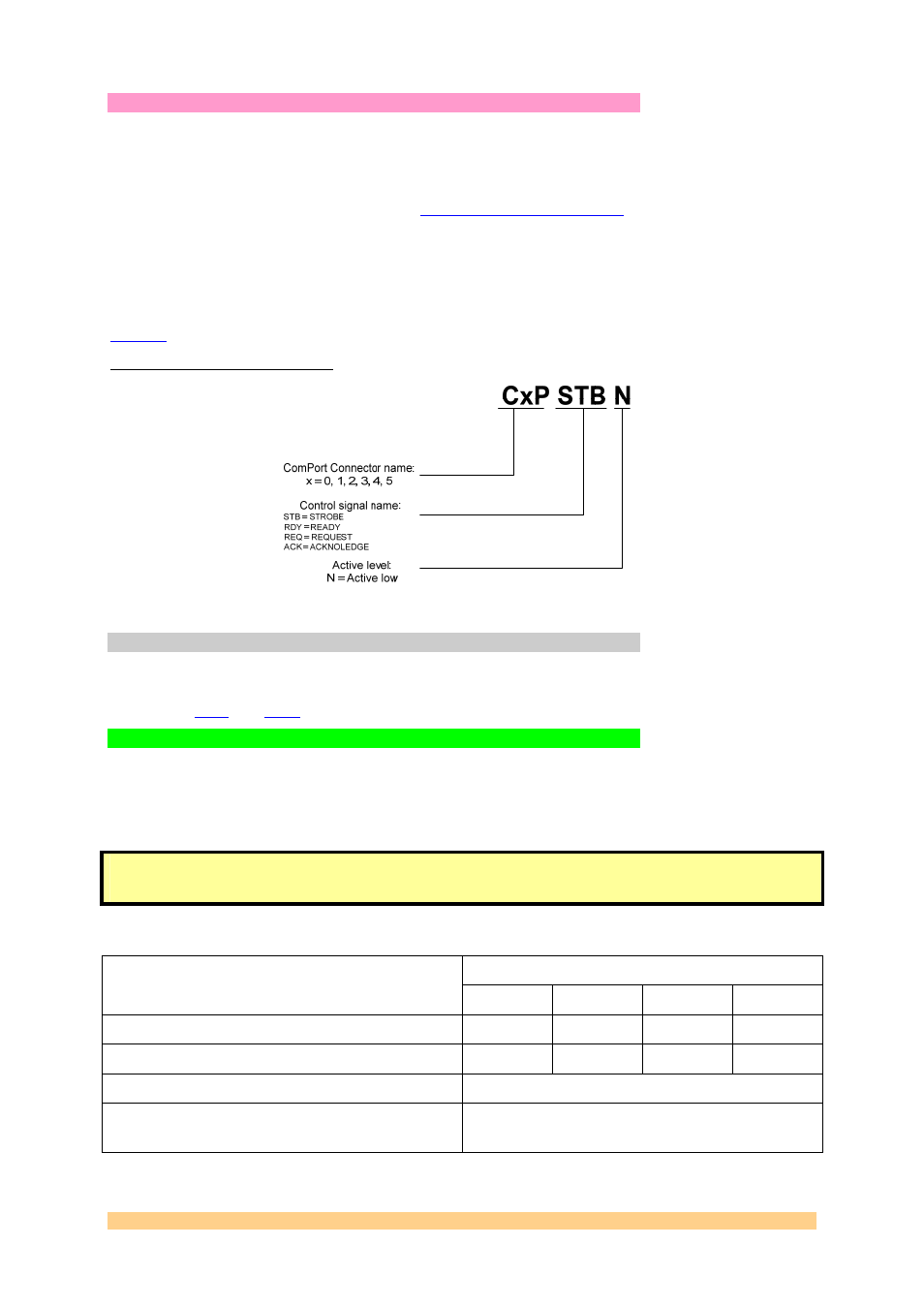
Constraints file signal names:
Figure 6: ComPort Constraints file signal names
4.1.10 DIP Switches
Two four-position DIP switches are connected to the CPLD: SW1 provides control over the
selection of the configuration bitstream source, and SW2 can be used as I/Os. They are
referenced
.
4.1.11 Clocking scheme
The SMT368 module provides an on-board oscillator and an external clock I/O:
• The on-board oscillator provides a free running clock to the FPGA and CPLD. The
default is a 50MHz oscillator, but other frequencies can be provided upon request to
Sundance.
Note: Please ask your Sundance technical or sale person when ordering if you
need other frequencies.
• An external clock input/output (J2) is provided directly to the FPGA via a 50 ohms
MMBX coax connector.
Specification
Description
V
IL
V
OL
V
IH
V
OH
Maximum voltage
0.8V 0.4V 3.8V
Minimum voltage
-0.5V 2.0V
2.4V
Impedance
50 ohms
Frequency
The frequency limitations are the ones of the
FPGA. Refer to the Xilinx’s user guide.
Table 1: External Clock specification
User Manual SMT368
Page 12 of 24
Last Edited: 31/12/2008 13:53:00