7 sundance high-speed bus, Sundance high-speed bus, Figure 3: zbt constraints file signal names – Sundance SMT368 User Manual
Page 10
The ZBTRAM is designed to sustain 100% bus bandwidth by eliminating turnaround cycle
when there is transition from Read to Write, or vice-versa.
The device is well suited for SDR applications that experience frequent bus turnarounds,
needs to operate on small data chunks (especially one-word chunks), and needs to operate at
higher frequencies than permitted by the flow-through version.
The memory is split in 2x18-bit-wide banks, and is expected to be clocked at 166MHz with a
speed grade -16.
The 2 banks present independent address/data and control busses.
To ensure high performance, the FPGA design should generate de-skewed controller and
board-level clocks using the clock feedback signal provided. The result is a high-speed, de-
skewed clock driving the controller and the ZBT SRAM.
For more complete information, please refer
and to Xilinx application note
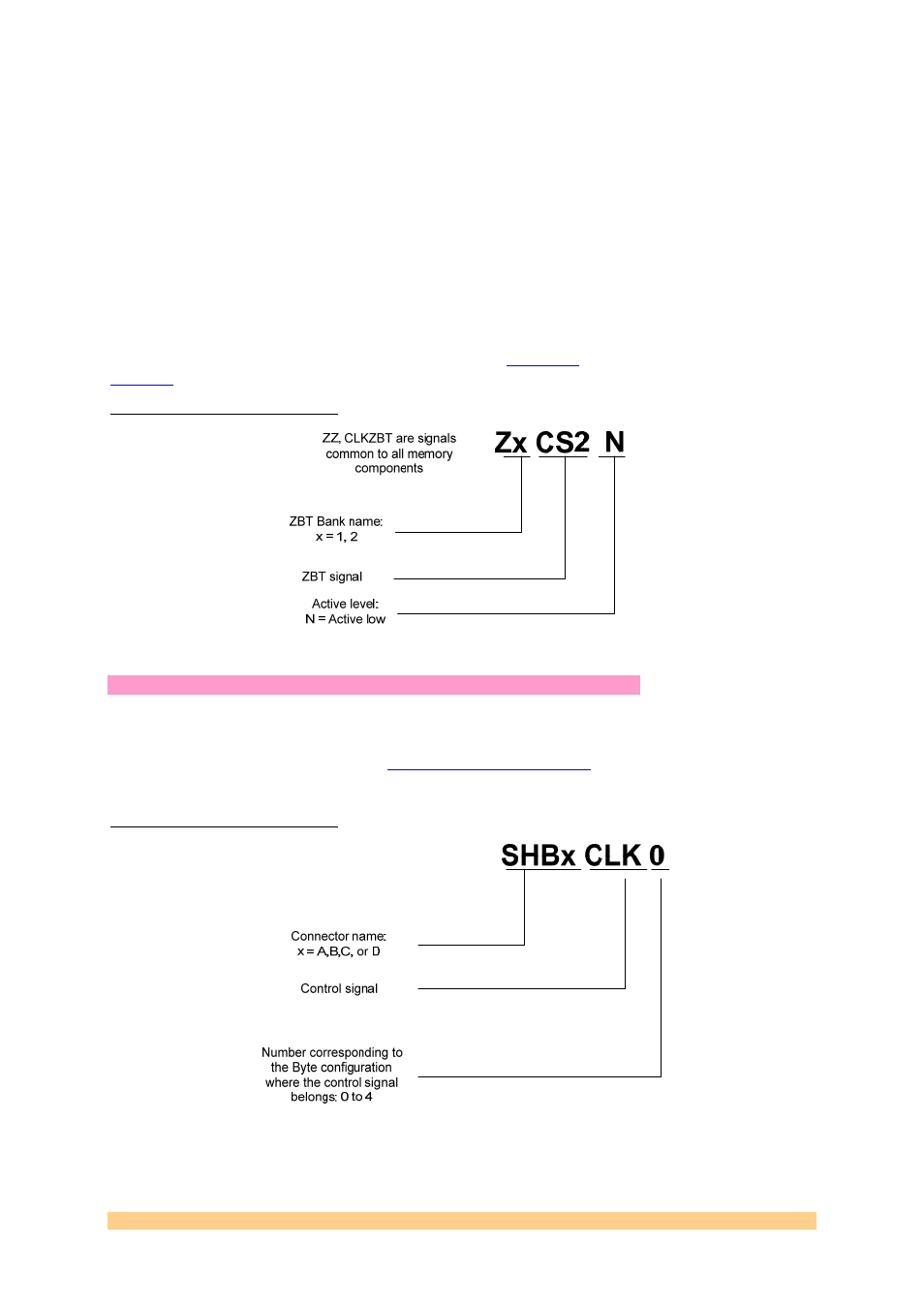
Constraints File signal names:
Figure 3: ZBT Constraints file signal names
4.1.7 Sundance High-speed bus
4 x 60-pin connectors provide 4 x 40 I/O connections between the FPGA and the outside
world. Note that there is no USER I/O pins implemented for the SHB.
The SHB interface is available in the
.
The FPGA I/O banks hosting the SHB signals are powered using Vcco=3.3V.
Constraints File signal names:
Figure 4: SHB Constraints file control signal names
User Manual SMT368
Page 10 of 24
Last Edited: 31/12/2008 13:53:00