Measurement Computing Digital488 User Manual
Page 21
Section 2
Getting Started
2.5
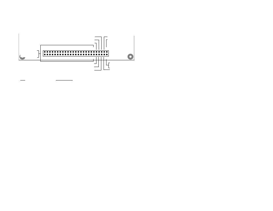
Digital488OEM I/O Connector Pin Out
External Data Ready (I)
Inhibit (O)
Data Strobe (O)
2
10
20
30
40
50
49
39
19
9
1
29
Clear (O)
Trigger (O)
Service (I)
+5 Volts
[ 50 mA Max!]
Not Used
Not Used
Common (GND)
(I)
(O)
= Input
= Output
Digital I/O
Bits 1 thru 40
PC Board Edge
Pin
Description
1 thru 8
DATA PORT1 (Input or Output).
Pin 1 is bit 1 (LSB), Pin 8 is bit 8 (MSB).
Least Significant Port
9 thru 16
DATA PORT2 (Input or Output).
Pin 9 is bit 1 (LSB), Pin 16 is bit 8 (MSB).
17 thru 24
DATA PORT3 (Input or Output).
Pin 17 is bit 1 (LSB), Pin 24 is bit 8 (MSB).
25 thru 32
DATA PORT4 (Input or Output).
Pin 25 is bit 1 (LSB), Pin 32 is bit 8 (MSB).
33 thru 40
DATA PORT5 (Input or Output).
Pin 33 is bit 1 (LSB), Pin 40 is bit 8 (MSB).
Most Significant Port
41
CLEAR (Output).
42
DATA STROBE (Output).
43
TRIGGER (Output).
44
INHIBIT (Output).