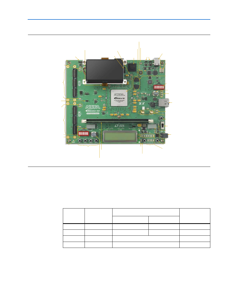
Figure 4–1 – Altera Stratix III User Manual
Page 16
4–2
Chapter 4: Development Board Setup
Powering Up the Board
Stratix III Development Kit User Guide
© August 2008
Altera Corporation
Before powering up, prepare the board as follows:
1. If cards are plugged into the HSMC ports, remove them.
2. Ensure that the POWER switch SW4 is in the OFF (or DOWN) position.
3. Configure the 8-position SW2 DIP switch to the default settings in
.
Figure 4–1. Stratix III Development Board Layout and Components
Stratix III
FPGA (U22)
MAX II
CPLD (U5)
Device Select (J2)
Jumper
24 MHz Crystal (Y2)
6 MHz
Crystal (Y3)
125 MHz MAX II Clock (Y1)
Type B USB
Connector (J5)
MAX II Control
DIP Switch (SW2)
Ethernet PHY
LEDs (D6, D7, D8) and
Duplex LED (D9)
PGM Config Select
Rotary Switch (SW3)
RJ-45 Ethernet
Connector (J14)
Clock In/Out SMAs (J16, J17)
Ethernet PHY TX/RX
Activity LEDs (D14, D15)
Factory Configuration
Push Button (S1)
Power Switch (SW4)
DC Power Jack (J21)
User Push Buttons
(S2 through S5)
Reset Configuration
Push Button (S7)
Configuration
Done LED (D32)
Board-Specific
LEDs (D33-D36)
User LEDs
(D20 through D27)
CPU Reset
Push Button (S6)
Flash Memory Device (U9)
24 MHz Crystal (Y4)
DDR2 SDRAM
(U17, U20)
DDR2 SDRAM
DIMM Connector (J19)
Power Select
Rotary Switch (SW6)
Power LED (D16)
HSMC Port A (J18)
HSMC Port B (J8)
HSMC Port A
Present LED (D17)
Power Display (U27)
User DIP Switch (SW5)
HSMC Port A
TX/RX Activity
LEDs (D11, D12)
HSMC Port B
Present LED (D10)
Speaker Header (J1)
HSMC Port B
TX/RX Activity LEDs
(D2, D3)
User Display (U28)
QDRII+ SRAM (U15)
(Behind the LCD Screen)
JTAG Control DIP Switch (SW1)
MSEL0 to GND
Jumper (J13)
Table 4–1. Switch SW2 Settings (Part 1 of 2)
Switch
Name
Function
Default
Position
Position 0
Position 1
1
mW/mA
mW
mA
0
2
V/W
V
W
1
3
RSV0
MAX_RESERVE0
X
4
RSV1
MAX_RESERVE1
X