Arduino connectors, Arduino connectors –7 – Altera MAX 10 FPGA User Manual
Page 19
Chapter 3: Board Components
3–7
Arduino Connectors
October 2014
Altera Corporation
MAX 10 FPGA (10M08S, 144-EQFP) Evaluation Kit
User Guide
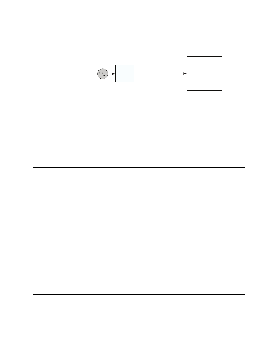
Figure 3–3
shows the general purpose clock going in to the evaluation kit.
Arduino Connectors
Arduino connectors J3, J4, and J5 connect to the MAX 10 FPGA. Any analog inputs
signals sourced through the Arduino header J4 are first filtered by the evaluation
boards op-amp based circuit. This circuit scales the maximum allowable voltage per
the Arduino specification (5.0V) to the maximum allowable voltage per the MAX 10
FPGA ADC IP block (2.5V).
Figure 3–3. MAX 10 FPGA (10M08S, 144-EQFP) Evaluation Kit General Purpose Clock
ICS8304
CLKBUF
MAX 10
FPGA
(U2)
50 MHz
Table 3–3. Arduino Connector Pin Assignments, Signal Names and Functions (Part 1 of 2)
Board
Reference
Schematic Signal Name
MAX 10 FPGA
Device Pin Number
Description
J3.1
ANALOG_VREF
5
Arduino analog Vref input
J3.2
GND
—
Arduino GND input
J3.3
ARDUINO_IO13
70
Arduino digital I/O input to FPGA
J3.4
ARDUINO_IO12
69
Arduino digital I/O input to FPGA
J3.5
ARDUINO_IO11
66
Arduino digital I/O input to FPGA
J3.6
ARDUINO_IO10
65
Arduino digital I/O input to FPGA
J3.7
ARDUINO_IO9
64
Arduino digital I/O input to FPGA
J3.8
ARDUINO_IO8
62
Arduino digital I/O input to FPGA
J4.1
ARDUINO_A0
6
Arduino analog channel input through the op-amp
filter circuit to the FPGA ADC IP input channel
ADCIN1
J4.2
ARDUINO_A1
7
Arduino analog channel input through the op-amp
filter circuit to the FPGA ADC IP input channel
ADC1IN2
J4.3
ARDUINO_A2
8
Arduino analog channel input through the op-amp
filter circuit to the FPGA ADC IP input channel
ADC1IN3
J4.4
ARDUINO_A3
10
Arduino analog channel input through the op-amp
filter circuit to the FPGA ADC IP input channel
ADC1IN4
J4.5
ARDUINO_A4
11
Arduino analog channel input through the op-amp
filter circuit to the FPGA ADC IP input channel
ADC1IN5