I/o address map, 9 i/o address map – ADLINK CM3-GF User Manual
Page 87
TME-104P-CMx-GF-1V7
Rev 1.7
79 (81)
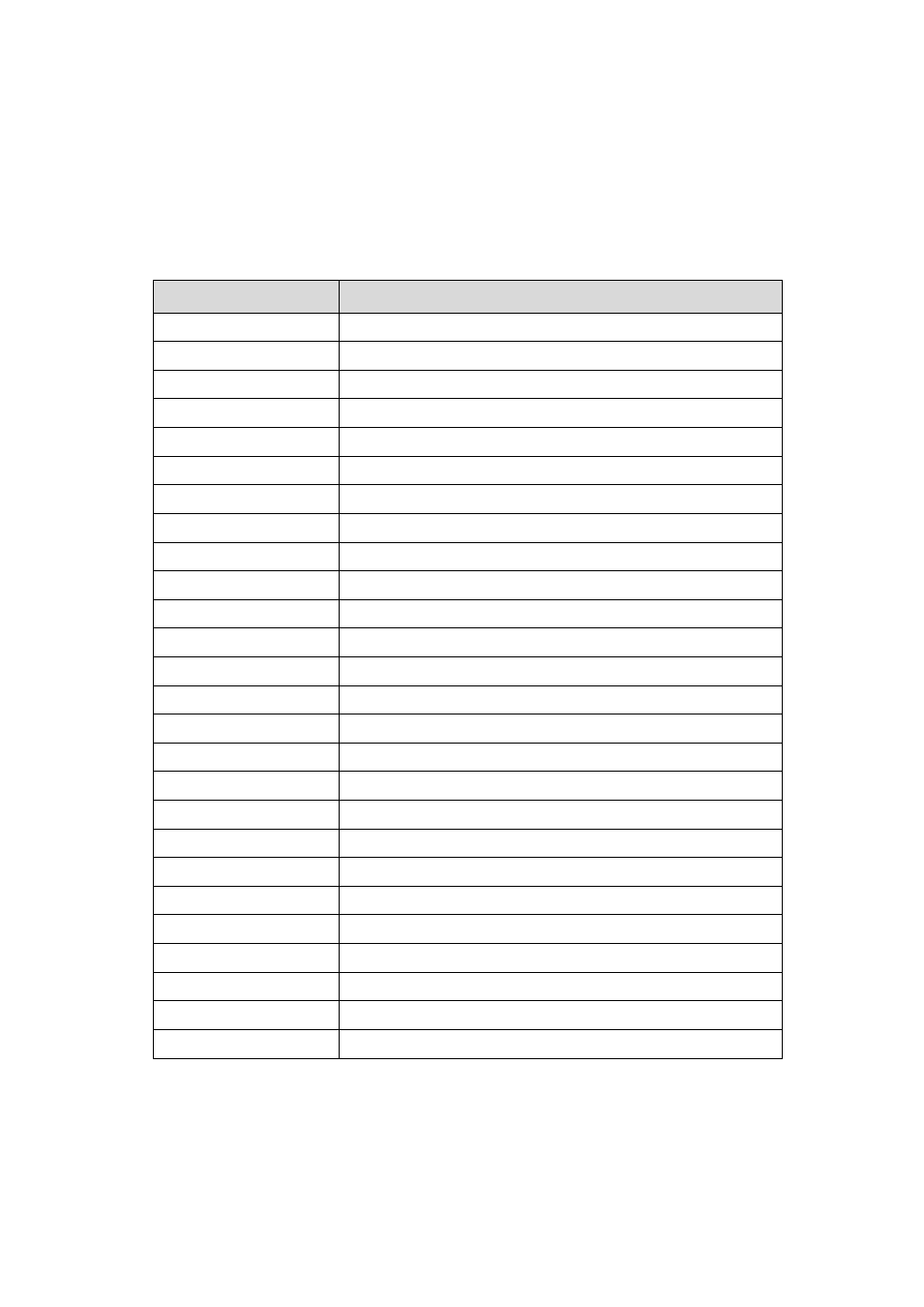
4.9 I/O Address Map
The system chipset implements a number of registers in I/O address space. These registers occupy the
following map in the I/O space:
Address range (hex)
Description
0000 - 000F
DMA controller
0020 - 0021
Programmable interrupt controller
002E - 002F
Super I/O
0040 - 0043
System timer
0048 - 004B
System timer
0060 - 0060
Keyboard
0061 - 0061
System speaker
0064 - 0064
Keyboard
0070 - 0073
System CMOS / Real-time clock
0080 – 0091
DMA controller
00A0 - 00A1
Programmable interrupt controller
00C0 - 00DF
DMA controller
00F0 - 00FF
Numeric co-processor
0170 – 0177
IDE controller
01F0 - 01F7
IDE controller
0203 – 020A
ISA-PnP data port
02F8 - 02FF
Serial port 2
0376
IDE controller
0378 - 037F
Parallel port
03B0 – 03BB
On-board VGA
03C0 – 03DF
On-board VGA
03F6
IDE controller
03F8 - 03FF
Serial port 1
04D0 - 04D1
PCI config space
0CF8 - 0CFF
PCI config space
1000 – 10FE
On-board VGA