6 data format, Data format – ADLINK PCI-9810 User Manual
Page 54
42
Operation Theory
5.6
Data Format
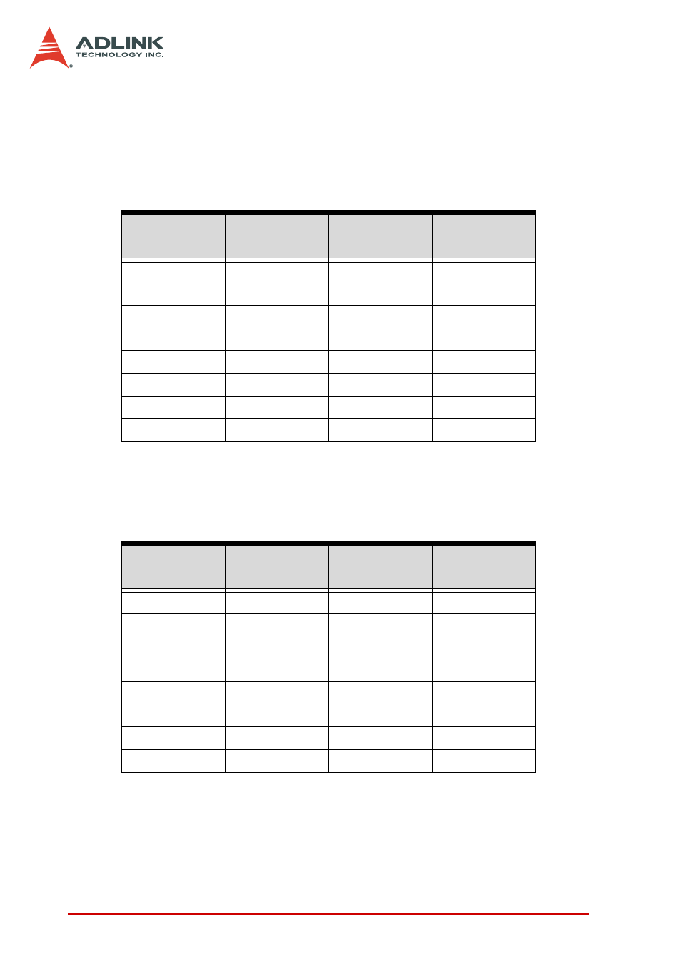
The A/D data of 12-bit PCI-9812 is on the 12 MSB of the 16-bit A/
D data. The 4 LSB of the 16-bit A/D data must be truncated by
software (Refer to section 6.2). The relationship between the real
signal voltage and the sampled value is shown below:
The A/D data of 10-bit PCI-9810 is on the 10 MSB of the A/D data.
The 6 LSB of the 16-bit A/D data must be truncated by software.
The relationship between the real signal voltage and the sampled
value is shown below:
A/D Data
(Hex)
Decimal
Value
V
(-1 V to +1 V)
V
(-5 V to +5 V)
7FF 0
+32752
+1.0000
+5.0000
400 0
+16384
+0.5002
+2.5010
001 0
+16
+0.0005
+0.0025
000 0
0
0.0000
0.0000
FFF 0
-16
0.0005
-0.0025
C00 0
-16384
-0.5002
-2.5010
801 0
-32752
-1.0000
-5.0000
800 0
-32768
-1.0049
-5.0024
A/D Data
(Hex)
Decimal
Value
V
(-1 V to +1 V)
V
(-5 V to +5 V)
7FC 0
+32704
+1.0000
+5.0000
400 0
+16384
+0.5002
+2.5010
0040
+64
+0.0005
+0.0025
000 0
0
0.0000
0.0000
FFC 0
-64
-0.0005
-0.0025
C00 0
-16384
-0.5002
-2.5010
804 0
-32704
-1.0000
-5.0000
800 0
-32768
-1.0020
-5.0098