Clock source register – ADLINK PCI-9810 User Manual
Page 39
Registers
27
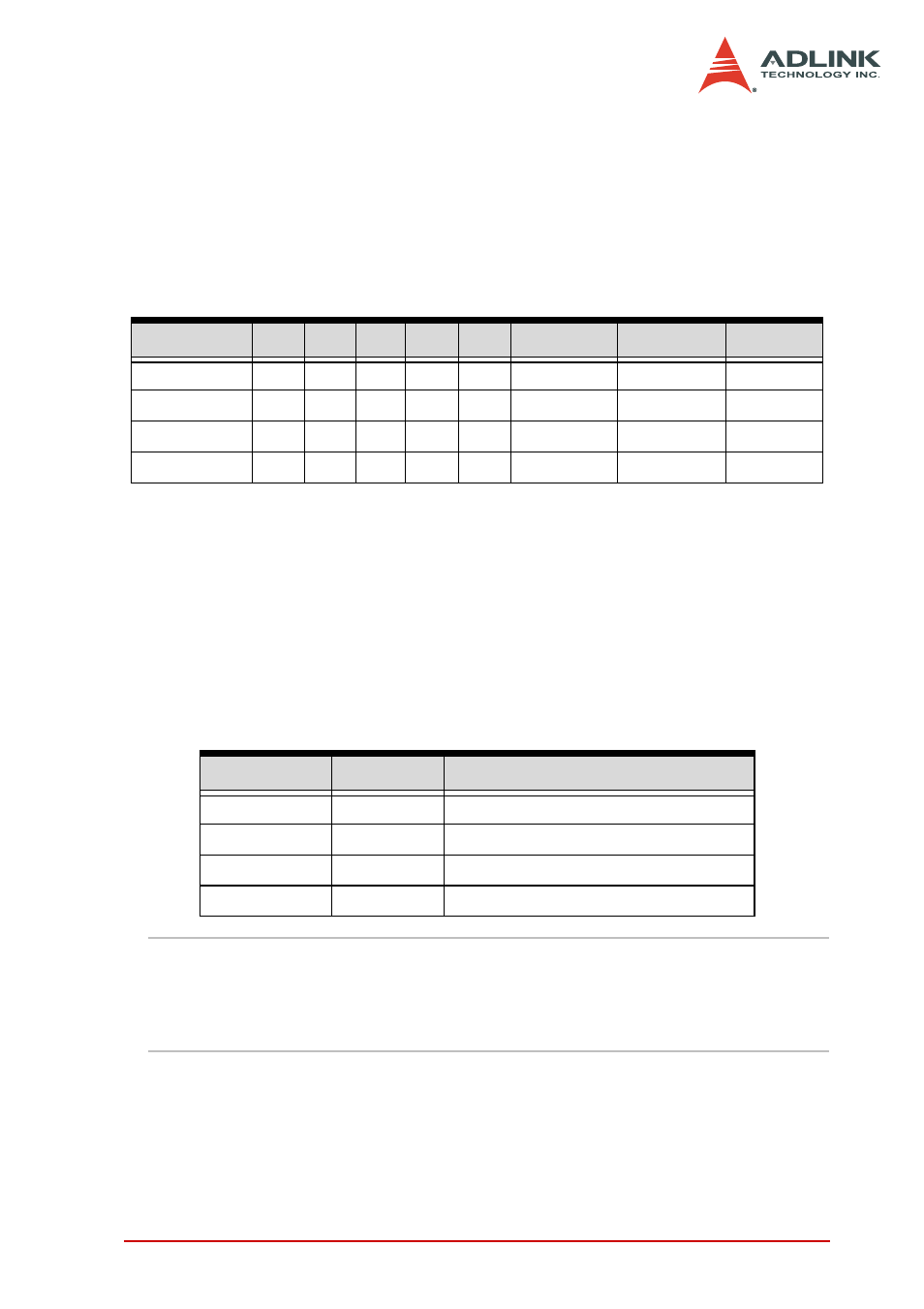
Clock Source Register
Selects the system clock source.
Address: BASE + 20h
Attribute: Write only
Data Format:
NOTE
When selected, the external clock is divided by the fre-
quency divider as mentioned. Thus, the frequency of the
external clock should be at least twice as the desired
sampling frequency.
Bit
7
6
5
4
3
2
1
0
BASE+18h
—
—
—
—
—
CLKSRC1 CLKSRC0 Freq_Sel
BASE+19h
—
—
—
—
—
—
—
—
BASE+1Ah
—
—
—
—
—
—
—
—
BASE+1Bh
—
—
—
—
—
—
—
—
Bit 31...3
Any value
Bit 2...1
CLKSRC1...0, ADC clock source
Bit 0
Freq_Sel: Frequency selection. Values include:
1: Frequency of A/D clock source is higher than the PCI clock
frequency (33 MHz)
0: Frequency of A/D clock source is lower than the PCI clock
frequency (33 MHz)
CLKSRC2
CLKSRC1
Selected clock source
0
0
Internal clock (40 MHz)
0
1
External sine wave clock
1
0
External digital clock
1
1
Illegal