Table 2-4: switches and resistors – ADLINK PCI-9810 User Manual
Page 25
Hardware Information
13
CAUTION
DO NOT leave the input connector unconnected when it
is configured as high impedance input. The input connec-
tor must be connected to a low impedance signal source
to provide a return path for the input bias current. Since
the OPAMP has a maximum input bias current of 35 µA
in the input stage, it will be placed in an abnormal envi-
ronment when the input is left unconnected and will lead
to saturation in the output stage. Although a current-limit-
ing resistor is present to protect the ADC, the large cur-
rent brought by the saturation will damage the ADC.
Offset problems will occur if you use high impedance
(~15 M
Ω) with signal sources having high output imped-
ance. The high output impedance and the input bias cur-
rent of up to 35 µA introduces a voltage drop of several
volts. Adjusting the variable resistor does not eliminate
this large offset voltage.
NOTE
75
Ω input impedance can be achieved by: (1) replacing
R95 with a 75-ohm resistor and close C0LO or (2) placing
a T-connector with a 75-ohm terminator on J1 and open
C0LO.
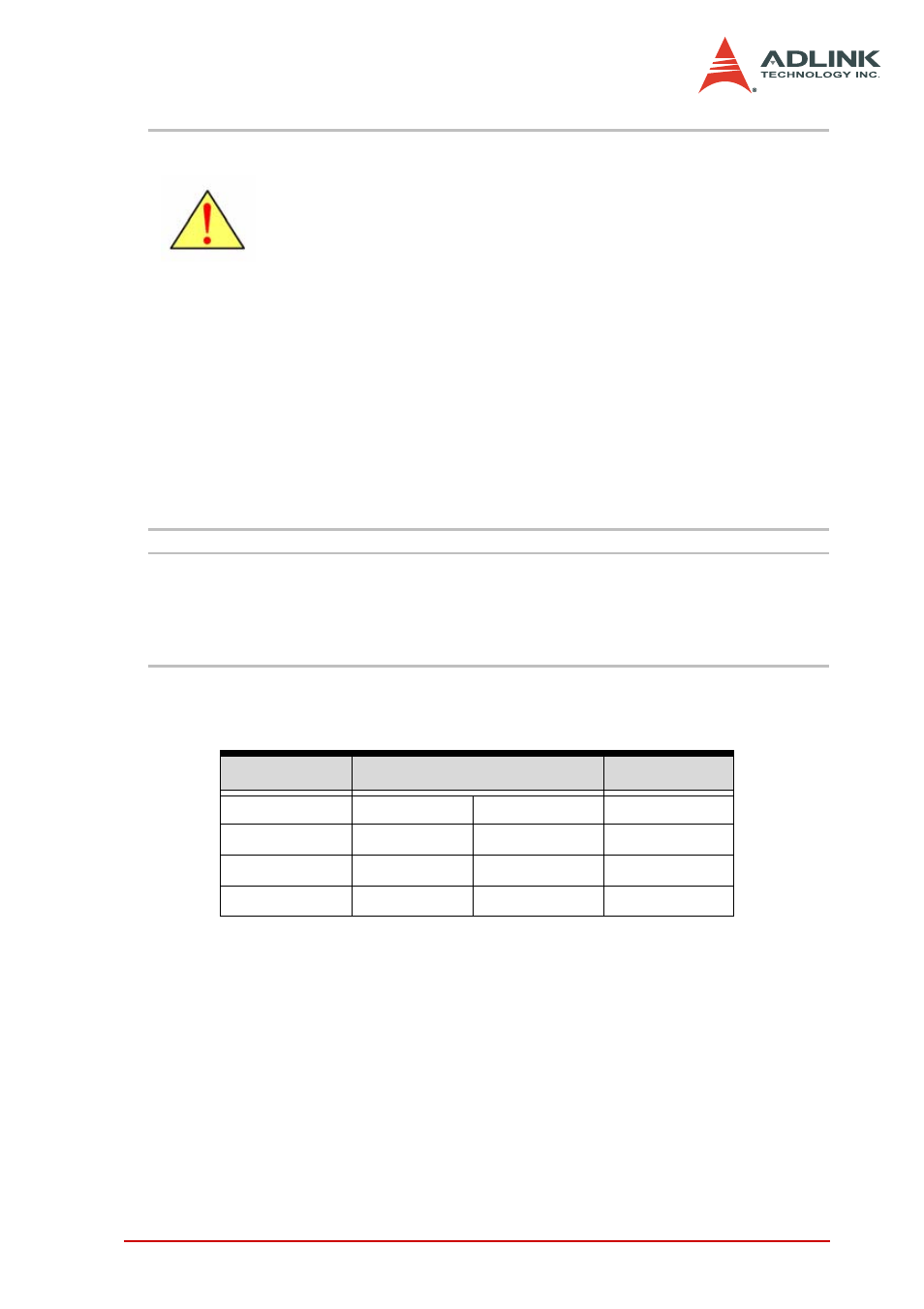
The corresponding switches and resistors of other channels are
listed below:
Channel
Switches
Resistor
Channel 0
C0LO
C05V
R95
Channel 1
C1LO
C15V
R96
Channel 2
C2LO
C25V
R97
Channel 3
C3LO
C35V
R98
Table 2-4: Switches and Resistors