4 registers, 1 i/o port address, I/o port address – ADLINK PCI-9810 User Manual
Page 29: Table 4-1: i/o address, 4registers
Registers
17
4
Registers
Descriptions of the register format and structure of the PCI-9812/
9810 are specified in this chapter. This information is for program-
mers that want to handle the card using low-level programming.
4.1
I/O Port Address
The PCI-9812/9810 functions as a 32-bit PCI target device to any
master on the PCI bus. It supports burst transfer to memory space
by using 32-bit data — where both data read and write are based
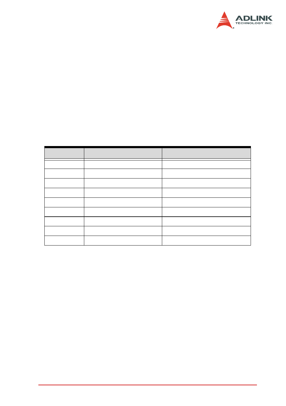
on 32-bit data transfer. Table 4-1 lists the I/O address of each reg-
ister according to the base address and the register function.
I/O Address
Read
Write
Base + 0
—
ADC Channel Enable Register
Base + 4
—
ADC Clock Divisor Register
Base + 8
—
Trigger Mode Register
Base + C
—
Trigger Level Register
Base + 10
—
Trigger Source Register
Base + 14
—
Post Trigger Counter Register
Base + 18
FIFO Control & Status Reg FIFO Control & Status Register
Base + 1C
—
Acquisition Enable Register
Base + 20
—
Clock Source Register
Table 4-1: I/O Address