Trigger level register – ADLINK PCI-9810 User Manual
Page 33
Registers
21
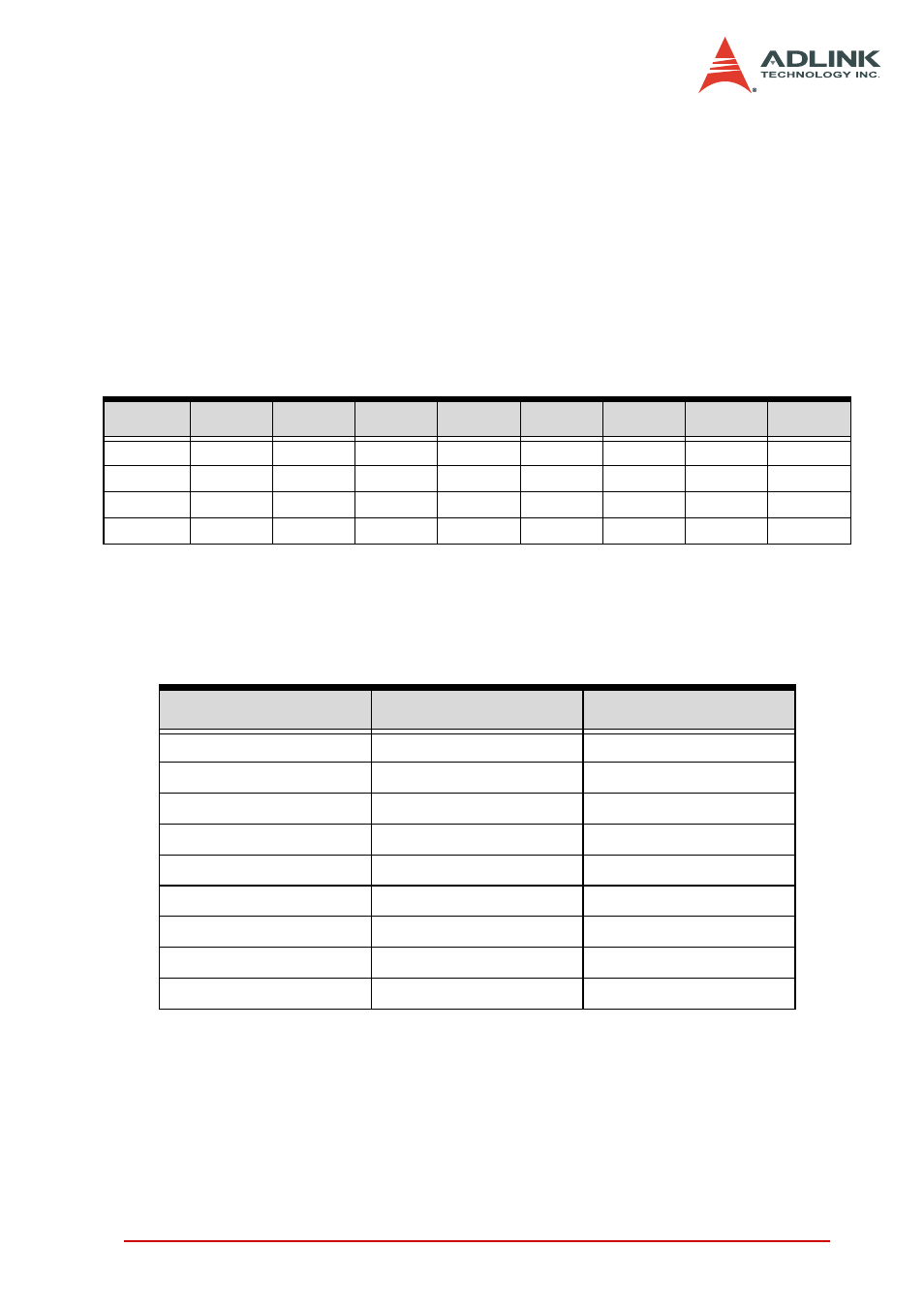
Trigger Level Register
The trigger condition of the PCI-9812/9810 includes a trigger level
and a trigger slope. This register sets the trigger level and the
trigger source register described in the next section, and sets the
trigger slope.
Address: BASE + 0ch
Attribute: Write only
Data Format:
Relationship between the 8-bit trigger level and the trigger voltage:
Bit
7
6
5
4
3
2
1
0
BASE+Ch
TRGLVL7
TRGLVL6
TRGLVL5
TRGLVL4
TRGLVL3
TRGLVL2
TRGLVL1
TRGLVL0
BASE+Dh
—
—
—
—
—
—
—
—
BASE+Eh
—
—
—
—
—
—
—
—
BASE+Fh
—
—
—
—
—
—
—
—
TRGLVL7...0
Trigger level
—
Any value
TRGLVL7..0(bit 7..0)
Trigger voltage(
±
1 V) Trigger voltage(
±
5 V)
0xFF
0.992 V
4.96 V
0xFE
0.984 V
4.92 V
|
|
|
0x81
0.008 V
0.04 V
0x80
0.000 V
0.00 V
0x7F
-0.008 V
-0.04 V
|
|
|
0x01
-0.992 V
-4.96 V
0x00
-1.000 V
-5.00 V
This manual is related to the following products: