4 pxi_clk10 clock, 5 pxi_clk100 clock, 6 adc timing control – ADLINK PXIe-9852 User Manual
Page 36: 1 timebase architecture, 2 basic acquisition timing, Pxi_clk10 clock, Pxi_clk100 clock, Adc timing control, Timebase architecture, Basic acquisition timing
26
Operations
3.5.4
PXI_CLK10 Clock
The PXIe-9852 can receive the timebase from the PXI_CLK10
Clock, the signal of which originates at the PXI Express chassis
backplane, matched in propagation delay within 1 ns.
3.5.5
PXI_CLK100 Clock
The PXIe-9852 can receive the timebase from the PXI_CLK100
Clock, the signal of which originates at the PXI Express chassis
backplane, matched in propagation delay within 200 ps.
3.6 ADC Timing Control
3.6.1
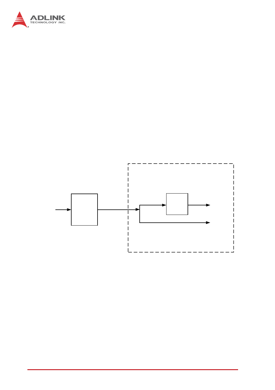
Timebase Architecture
Figure 3-11: PXIe-9852 Timebase Architecture
3.6.2
Basic Acquisition Timing
The PXIe-9852 commences acquisition upon receipt of a trigger
event originating with software command, external digital trigger,
or the PXIe Trigger Bus. The Timebase is a clock provided to the
ADC and acquisition engine for essential timing. The Timebase is
ADC
ADC Output
Onboard
200 MHz
Oscillator
200 MHz
X2
Multiplier
PLL
400 MHz
200 MHz
FPGA
For ADC
Data Bus
For ADC
state
machine