3 operations, 1 functional block diagram, 2 analog input channel – ADLINK PXIe-9852 User Manual
Page 25: 1 analog input front-end configuration, Functional block diagram, Analog input channel, Analog input front-end configuration, Figure 3-1, Analog input architecture of the pxie-9852, 3operations
Operations
15
PXIe-9852
3
Operations
This chapter contains information regarding analog input, trigger-
ing and timing for the PXIe-9852.
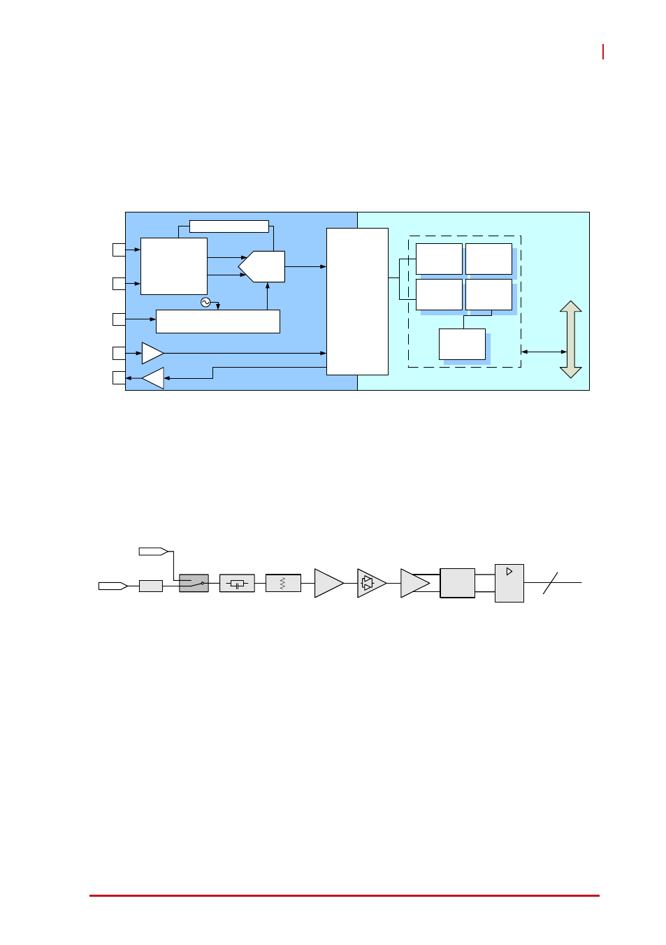
3.1 Functional Block Diagram
3.2 Analog Input Channel
3.2.1
Analog Input Front-End Configuration
Figure 3-1: Analog Input Architecture of the PXIe-9852
Input Configuration
The input channel terminates with equivalent 50Ω or 1 MΩ
input impedance (selected by software). The 14-bit ADC pro-
vides not only accurate DC performance but also high signal-
to-noise ratio, and high spurious-free dynamic range in AC per-
formance. The ADC transfers data to system memory via the
high speed PCI Express Gen2 X 4 interface.
For auto-calibration, internal calibration provides stable and
accurate reference voltage to the AI.
CH0
CH1
CLK IN
TRG IN
Analog Front End
14 bit ADC
buffer
Synthesizer
B to B
High Speed
Interface
Daughter Board
Carrier Board
Calibration CKT
ADC
Interface
Trigger
Interface
FIFO
Local Bus
Interface
PXI Express
Controller
FPGA
PXI E
x
pr
ess BU
S
TRG OUT
buffer
Protection ckt
Calibration Source
AC / DC
Couple
High Impedance
Buffer
50
/ Hi-Z
1x / 10x
amplifier
ADC Driver
100MHz
LPF
0
0
0
0
0
14
14-bit ADC