2 input range and data format, 3 dma data transfer, Input range and data format – ADLINK PXIe-9852 User Manual
Page 26: Dma data transfer
16
Operations
3.2.2
Input Range and Data Format
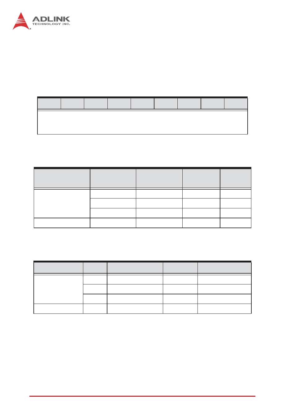
Data format of the PXIe-9852 is 2’s complement. The ADC data of
PXIe-9852 is on the 14 MSB of the 16-bit A/D data. The 2 LSB of
the 16-bit A/D data should be truncated by software. A/D data
structure is as follows.
Table 3-1: Input Range and Data Format
Table 3-2: Input Range FSR and –FSR Values
Table 3-3: Input Range Midscale Values
3.2.3
DMA Data Transfer
The PXIe-9852, a PCIe Gen 2 X 4 device, is equipped with a
200MS/s high sampling rate ADC, generating a 800 MByte/
second rate.
D15
D14
D13
D12
….
D3
D2
D1
D0
D15 ~ D2 bits represent the data from ADC (2’s complement)
D1, D0 bits are always 0.
Description
Full scale
range
Least
significant bit
FSR-1LSB
-FSR
Bipolar Analog
Input
±10V
1.22mV
9.99878V
-10.000V
±2V
0.244mV
1.99976V
-2V
±0.2V
24.4uV
0.199976V
-0.2V
Digital Code
N/A
N/A
7FFC
8000
Description
Midscale +1LSB
Midscale
Midscale -1LSB
Bipolar Analog
Input
±10V
1.22mV
0V
-1.22mV
±2V
0.244mV
0V
-0.244mV
±0.2V
24.4V
0V
-24.4μV
Digital Code
0004
0000
FFFC