Table 1-4: trigger bus switch functions, Figure 1-9, Trigger bus switching – ADLINK PXIS-2719A User Manual
Page 24

14
Introduction
the second from slot 7 to slot 12, and the last from slot 13 to slot
19. Switch SWY1 shown is the on-board switch, controlling the
configuration of these two buffers.
Table 1-4: Trigger Bus Switch Functions
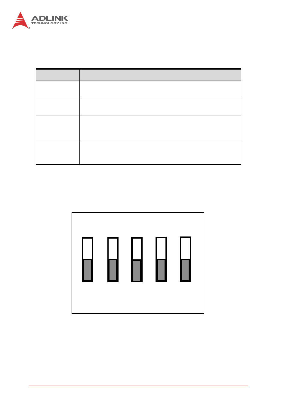
Figure 1-9: Trigger Bus Switching
Switch
Function
P2 on switch
Enables/Disables (On/Off) bus buffer between first and
second segments
P3 on switch
Enables/Disables (On/Off) bus buffer between second
and third segments
P4 on switch
Determines direction of the bus buffer between first and
second segments, with high left to right and low right to
left
P5 on switch
Determines direction of the bus buffer between second
and third segments, with high left to right and low right to
left
P1 P2 P3 P4 P5
ON
1
2
3
4
5
See also other documents in the category ADLINK Hardware:
- USB-1901 (84 pages)
- USB-1210 (54 pages)
- USB-2401 (60 pages)
- USB-7230 (50 pages)
- USB-2405 (56 pages)
- DAQe-2010 (92 pages)
- DAQe-2204 (100 pages)
- DAQe-2213 (94 pages)
- DAQe-2501 (74 pages)
- PXI-2010 (84 pages)
- PXI-2020 (60 pages)
- PXI-2501 (62 pages)
- cPCI-9116 (98 pages)
- ACL-8112 Series (93 pages)
- ACL-8112 Series (94 pages)
- ACL-8112 Series (92 pages)
- ACL-8216 (75 pages)
- ACL-8111 (61 pages)
- PCM-9112+ (10 pages)
- PCM-9112+ (94 pages)
- cPCI-6216V (47 pages)
- ACL-6126 (28 pages)
- ACL-6128A (40 pages)
- PCM-6308V+ (4 pages)
- PCM-6308V+ (52 pages)
- PCI-7444 (82 pages)
- PCI-7434 (48 pages)
- PCI-7234 (56 pages)
- PCI-7260 (66 pages)
- PCI-7258 (38 pages)
- PCI-7256 (48 pages)
- PCI-7250 (48 pages)
- LPCI-7250 (48 pages)
- PCI-7396 (65 pages)
- PCI-7296 (59 pages)
- PCI-8554 (67 pages)
- PCIe-7360 (94 pages)
- PCIe-7350 (86 pages)
- PCIe-7300A (114 pages)
- PCIe-7200 (51 pages)
- PCI-7300A (112 pages)
- PCI-7300A (83 pages)
- PCI-7200 (96 pages)
- cPCI-7300 (82 pages)
- cPCI-7300 (83 pages)
