2 timer/counter registers, 3 chip select register – ADLINK ACL-8454/12 User Manual
Page 33

Registers Format
• 25
3.2 Timer/Counter
Registers
Every 8254 occupies 4 I/O address locations in the ACL-8454 as shown
below. Condensed information is specified in Appendix B Timer/Counter
Operation. Users can refer to Tundra’s website (“http://www.tundra.com”) or
Intel's data sheet for a fully descriptions of the 8254 features (see
“http://support.intel.com/support/controllers/peripheral/231164.htm”). Note
that only one 8454 chip can be enabled at the same time.
Address : BASE + 0 ~ BASE + 3
Attribute : read / write
Data Format :
Base + 0
Counter 0 Register ( R/W)
Base + 1
Counter 1 Register ( R/W)
Base + 2
Counter 2 Register ( R/W)
Base + 3
8254 Mode Control Register (W)
8254 Read Back Register (R)
3.3 Chip
Select
Register
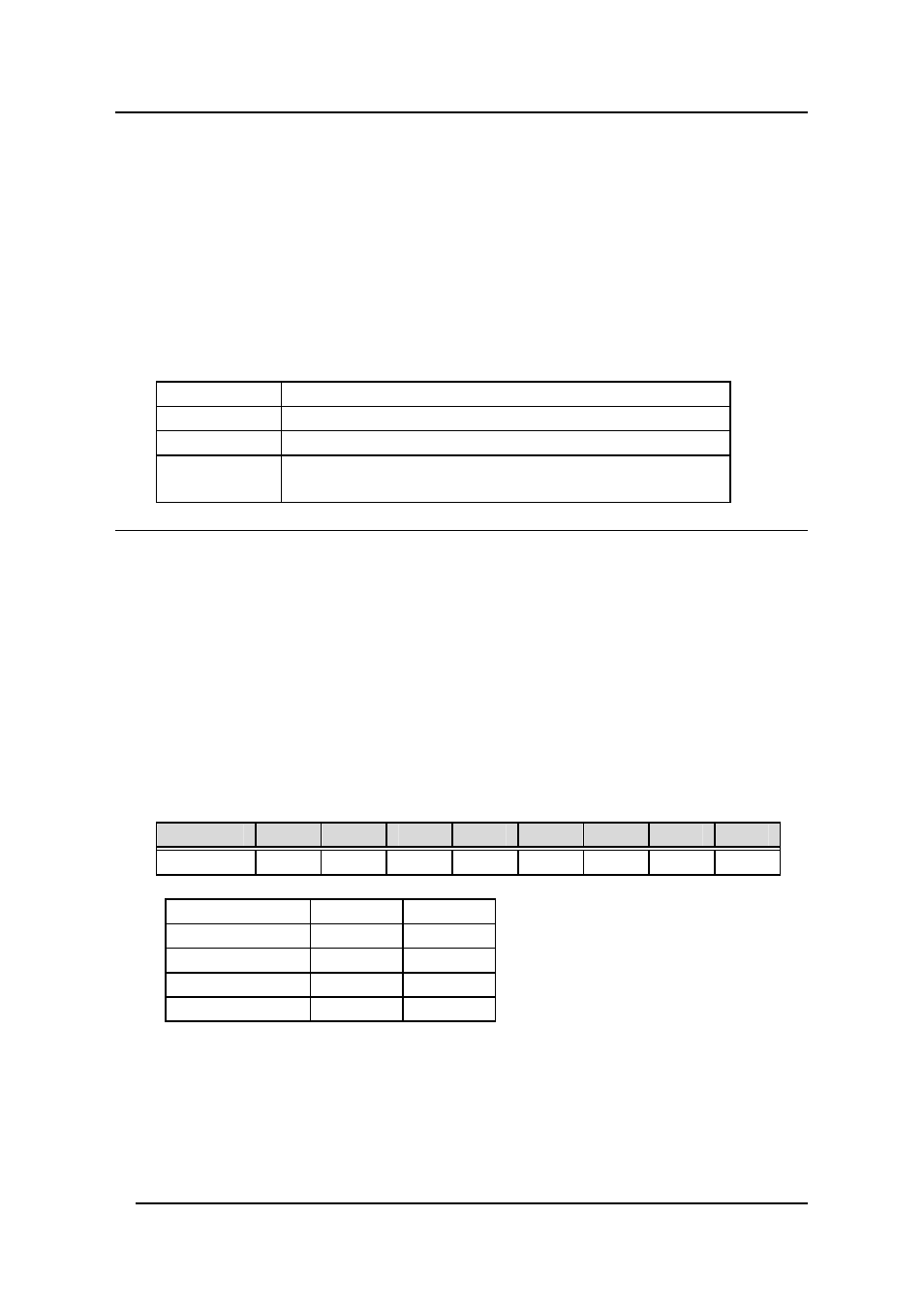
Although there are at most four 8254 chips can be installed on board,
however, only one 8254 can be selected at the same time. The bits 0, 1 of
the chip select register (CS1 and CS0) are used to select 8254 chips.
Whenever a chip is selected (active), the 8254 I/O address (BASE+0 ~
BASE+3) is selected by this chip. The active chip is enabled by CS0 and
CS1 according the following table.
Address : BASE + 4
Attribute : write only
Data Format :
Bit
7
6
5
4
3
2
1
0
Base
+
4
-- -- -- -- -- --
CS1
CS0
8254 Chip #
CS1
CS0
Chip #1
0 0
Chip #2
0 1
Chip #3
1 0
Chip #4
1 1
