5 digital input register – ADLINK PCI-8554 User Manual
Page 38
28 • Registers
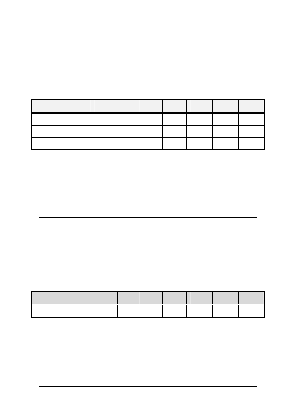
There are a total of twenty-two bits on the cPCI/PCI-8554/R used for
selecting clock sources for Timer/Counter 1 ~ 10, CK1 and the debounce
system.
Address: BASE + 0x10 ~ 0x12
Attribute: write only
Data Format:
Bit
7
6
5
4
3
2
1
0
Base+0x10 C4N2
C4N1 C3N2 C3N1
C2N2 C2N1 C1N2 C1N1
Base+0x11 C8N2
C8N1 C7N2 C7N1
C6N2 C6N1 C5N2 C5N1
Base+0x12 - DBCSEL
- CK1SEL
C10N2 C10N1
C9N2 C9N1
Table 6. Timer/Counter Clock Mode Control Register
CnN1and CnN2:
These two bits are used to control clock source of
Timer/Counter n, n = 1 ~ 10
CK1SEL:
select source of CK1
DBCSEL:
select debounce clock
3.5
Digital Input Register
There are 8 digital input channels on the cPCI/PCI-8554/R.
Address: BASE + 0x18
Attribute: read only
Data Format:
Bit
7
6
5
4
3
2
1
0
Base+0x18 DI7 DI6 DI5 DI4 DI3 DI2 DI1 DI0
Table 7. Digital Input Register
- USB-1901 (84 pages)
- USB-1210 (54 pages)
- USB-2401 (60 pages)
- USB-7230 (50 pages)
- USB-2405 (56 pages)
- DAQe-2010 (92 pages)
- DAQe-2204 (100 pages)
- DAQe-2213 (94 pages)
- DAQe-2501 (74 pages)
- PXI-2010 (84 pages)
- PXI-2020 (60 pages)
- PXI-2501 (62 pages)
- cPCI-9116 (98 pages)
- ACL-8112 Series (93 pages)
- ACL-8112 Series (94 pages)
- ACL-8112 Series (92 pages)
- ACL-8216 (75 pages)
- ACL-8111 (61 pages)
- PCM-9112+ (10 pages)
- PCM-9112+ (94 pages)
- cPCI-6216V (47 pages)
- ACL-6126 (28 pages)
- ACL-6128A (40 pages)
- PCM-6308V+ (52 pages)
- PCM-6308V+ (4 pages)
- PCI-7444 (82 pages)
- PCI-7434 (48 pages)
- PCI-7234 (56 pages)
- PCI-7260 (66 pages)
- PCI-7258 (38 pages)
- PCI-7256 (48 pages)
- PCI-7250 (48 pages)
- LPCI-7250 (48 pages)
- PCI-7396 (65 pages)
- PCI-7296 (59 pages)
- PCIe-7360 (94 pages)
- PCIe-7350 (86 pages)
- PCIe-7300A (114 pages)
- PCIe-7200 (51 pages)
- PCI-7300A (83 pages)
- PCI-7300A (112 pages)
- PCI-7200 (96 pages)
- cPCI-7300 (82 pages)
- cPCI-7300 (83 pages)