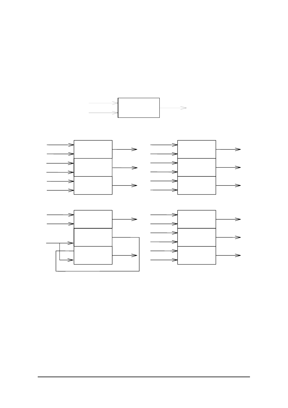
Figure 7: default counters architectural – ADLINK PCI-8554 User Manual
Page 26

16 • Getting Started
There are three signals (2 input and 1 output) for each counter, a clock
input signal, a gate control signal, and an output signal. Figure 6
illustrates the block diagram of the 8254 counter. CLK1 ~ CLK12 are
clock sources, GATE1 ~ GATE12 are gate control signals and COUT1 ~
COUT12 are outputs of the counters. Figure 7 shows the inter-connection
of the 8254 counters and the labels associated to each counter.
Clock Source Input
Counter / Timer Output
Gate Control Input
Counter
8254 Chip
C
G
O
Figure 6: Block Diagram of 8254 Counter
CLK1
COUT1
GATE1
Counter #1
CLK2
COUT2
GATE2
Counter #2
CLK3
COUT3
GATE3
Counter #3
8254 Chip #1
CLK4
COUT4
GATE4
Counter #4
Counter #5
COUT6
Counter #6
8254 Chip #2
CLK7
COUT7
GATE7
Counter #7
CLK8
COUT8
GATE8
Counter #8
CLK9
COUT9
GATE9
Counter #9
8254 Chip #3
CLK10
COUT10
GATE10
Counter #10
COUT11
COUT12
Counter #12
8254 Chip #4
Counter #11
C
G
O
C
G
C
G
C
G
C
G
C
G
C
G
C
G
C
G
C
G
C
G
C
G
O
O
O
O
O
O
O
O
O
O
O
8M Hz
CLK5
GATE5
CLK6
GATE6
COUT5
VCC
Figure 7: Default Counters Architectural
