ADLINK PCI-7396 User Manual
Page 33
Operation Theorem
• 25
4.2 8254 Timer/Counter Operation
4.2.1
Introduction
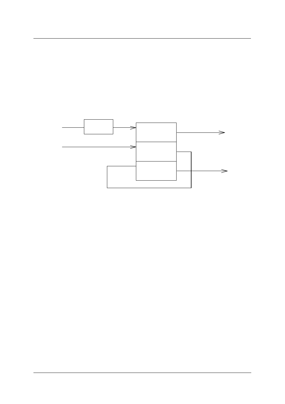
One 8254 programmable timer/counter chip is installed in the PCI-7396.
There are three counters in one 8254 chip and 6 possible operation modes
for each counter. The block diagram of the timer /counter system is shown in
Figure 4.3.
Event IRQ
Counter #0
2 MHz Clock
Timer #1
Timer IRQ
Timer #2
8254 Chip
Gate='H'
Gate='H'
Gate='H'
EVENT
(PIN 51)
Event Edge
Control
Figure 4.3 Timer / counter system of PCI-7396.
Timer #1 and timer #2 of the 8254 chip are cascaded as a 32-bits
programmable timer. In the software library, timer #1 and #2 are always set
as mode 2 (rate generator). Counter #0 is used as an event counter, that is,
there is an interrupt on the terminal count of 8254 mode 0.
4.2.2
Cascaded 32 bits Timer
The base frequency of input clock for the cascaded timer is 2MHz. The
output is send to be the timer interrupt. To set the maximum and minimum
frequency of the timer, please refer to the function _7348_Cascaded_Timer
or _7396_Cascaded_Timer.
4.2.3
Event Counter and Edge Control
The counter #0 of 8254 is used to be an event counter. The input is pin-51
of CN1. The trigger edge of counter clock is programmable. The gate
control fixs high (enable). The output is send to be the event interrupt. That
means If counter #0 is set as 8254 mode 0, the event IRQ asserts as the
counter counts down to zero.