ADLINK PCI-7396 User Manual
Page 20
12
• Installation
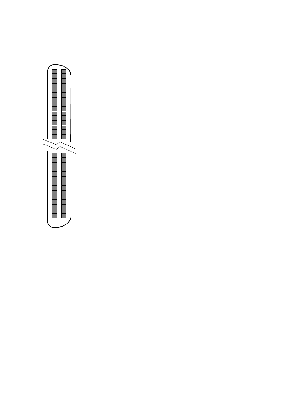
2.6 Connectors’ Pin Assignment of PCI-7396
(1)
(2)
(3)
(52)
(53)
(51)
(48)
(49)
(50)
(98)
(99)
(100)
Figure 2.3 Connectors Pin Assignment of PCI-7396
The DIO pin names are specified as PnXb, where
n : means the PPI number of the PCI-7396, n=1~4
X : means the port name of the PPI, X= ‘A’ , ‘B’ or ‘C’
b: means the bit number of the port, b=0~7
For example, P1C4 means bit 4 of port C on PPI1.
EXTTRG : External trigger signal to latch digital input data
EVENT : External event source for counter 0
GND : Ground
(1) P1A0 (26) P2A0 (51) P3A0/EVENT (76) P4A0
(2) P1A1 (27) P2A1 (52) P3A1 (77) P4A1
(3) P1A2 (28) P2A2 (53) P3A2 (78) P4A2
(4) P1A3 (29) P2A3 (54) P3A3 (79) P4A3
(5) P1A4 (30) P2A4 (55) P3A4 (80) P4A4
(6) P1A5 (31) P2A5 (56) P3A5 (81) P4A5
(7) P1A6 (32) P2A6 (57) P3A6 (82) P4A6
(8) P1A7 (33) P2A7 (58) P3A7 (83) P4A7
(9) P1B0 (34) P2B0 (59) P3B0 (84) P4B0
(10) P1B1 (35) P2B1 (60) P3B1 (85) P4B1
(11) P1B2 (36) P2B2 (61) P3B2 (86) P4B2
(12) P1B3 (37) P2B3 (62) P3B3 (87) P4B3
(13) P1B4 (38) P2B4 (63) P3B4 (88) P4B4
(14) P1B5 (39) P2B5 (64) P3B5 (89) P4B5
(15) P1B6 (40) P2B6 (65) P3B6 (90) P4B6
(16) P1B7 (41) P2B7 (66) P3B7 (91) P4B7
(17) P1C0 (42) P2C0 (67) P3C0 (92) P4C0
(18) P1C1 (43) P2C1 (68) P3C1 (93) P4C1
(19) P1C2 (44) P2C2 (69) P3C2 (94) P4C2
(20) P1C3 (45) P2C3 (70) P3C3 (95) P4C3
(21) P1C4 (46) P2C4 (71) P3C4 (96) P4C4
(22) P1C5 (47) P2C5 (72) P3C5 (97) P4C5
(23) P1C6 (48) P2C6 (73) P3C6 (98) P4C6
(24) P1C7 (49) P2C7 (74) P3C7 (99) P4C7/EXTTRG
(25) GND (50) GND (75) GND (100) GND