3 digital data registers – ADLINK PCI-7396 User Manual
Page 26
18
• Registers Format
The PCI-7396 has 2/4 PPIs on board. Each PPI contains 5 registers,
including Digital Data Register, Control Register, External Trigger Enable
Register, External Trigger Disable Register, and COS Interrupt Control
Register.
In the following sections, the 5 registers of PPI1 will be introduced
respectively. The registers of the other 3 PPIs are of the same configuration
which will not be repeated in this manual.
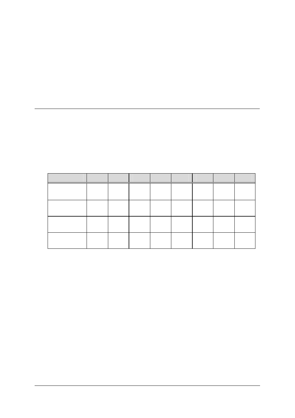
3.3 Digital Data Registers
The 24-bit I/O data of the PCI-7396 is accessed from/to this register by
software. The digital data can also be read back through this register.
Address: BASE + 00h
Attribute: read and write
Data Format:
Bit
7
6
5
4
3
2
1
0
BASE+
00h
P1A
7
P1A
6
P1A
5
P1A
4
P1A
3
P1A
2
P1A
1
P1A
0
BASE+
01h
P1B
7
P1B
6
P1B
5
P1B
4
P1B
3
P1B
2
P1B
1
P1B
0
BASE+
02h
P1C
7
P1C
6
P1C
5
P1C
4
P1C
3
P1C
2
P1C
1
P1C
0
BASE+
03h
X
X
X
X
X
X
X
X
P1X7~P1X0: Digital I/O data X:A~C.
- USB-1901 (84 pages)
- USB-1210 (54 pages)
- USB-2401 (60 pages)
- USB-7230 (50 pages)
- USB-2405 (56 pages)
- DAQe-2010 (92 pages)
- DAQe-2204 (100 pages)
- DAQe-2213 (94 pages)
- DAQe-2501 (74 pages)
- PXI-2010 (84 pages)
- PXI-2020 (60 pages)
- PXI-2501 (62 pages)
- cPCI-9116 (98 pages)
- ACL-8112 Series (92 pages)
- ACL-8112 Series (93 pages)
- ACL-8112 Series (94 pages)
- ACL-8216 (75 pages)
- ACL-8111 (61 pages)
- PCM-9112+ (10 pages)
- PCM-9112+ (94 pages)
- cPCI-6216V (47 pages)
- ACL-6126 (28 pages)
- ACL-6128A (40 pages)
- PCM-6308V+ (52 pages)
- PCM-6308V+ (4 pages)
- PCI-7444 (82 pages)
- PCI-7434 (48 pages)
- PCI-7234 (56 pages)
- PCI-7260 (66 pages)
- PCI-7258 (38 pages)
- PCI-7256 (48 pages)
- PCI-7250 (48 pages)
- LPCI-7250 (48 pages)
- PCI-7296 (59 pages)
- PCI-8554 (67 pages)
- PCIe-7360 (94 pages)
- PCIe-7350 (86 pages)
- PCIe-7300A (114 pages)
- PCIe-7200 (51 pages)
- PCI-7300A (112 pages)
- PCI-7300A (83 pages)
- PCI-7200 (96 pages)
- cPCI-7300 (82 pages)
- cPCI-7300 (83 pages)