ADLINK PCI-7396 User Manual
Page 19
Installation
• 11
2.5 Connectors’ Pin Assignment of PCI-7348
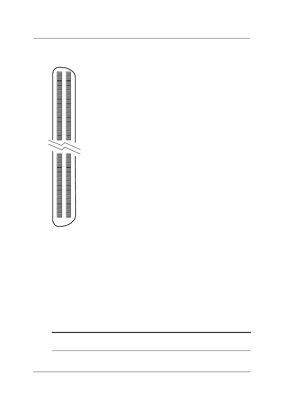
The I/O pin assignment of PCI-7348 is shown in the Figure 2.2.
The DIO pin names are specified as PnXb, where
n : means the PPI number of the PCI-7348, n=1~2
X : means the port name of the PPI, X= ‘A’ , ‘B’ or ‘C’
b: means the bit number of the port, b=0~7
For example, P1C4 means bit 4 of port C on PPI1.
EXTTRG : External trigger signal to latch digital input data
EVENT
: External event source for counter 0
V5V
: +5V power supply output
+12V
: +12v power supply output
GND
: Ground
Note : The power supply pins are protected by resettable fuses. Refer
to section 4.4 for details of the power supply.
(1)
(2)
(3)
(52)
(53)
(51)
(48)
(49)
(50)
(98)
(99)
(100)
(1)
P1A0 (26) P2A0
(51) EVENT
(76) GND
(2)
P1A1 (27) P2A1
(52) GND
(77) GND
(3)
P1A2 (28) P2A2
(53) GND
(78) GND
(4)
P1A3 (29) P2A3
(54) GND
(79) GND
(5)
P1A4 (30) P2A4
(55) GND
(80) GND
(6)
P1A5 (31) P2A5
(56) GND
(81) GND
(7)
P1A6 (32) P2A6
(57) GND
(82) GND
(8)
P1A7 (33) P2A7
(58) GND
(83) GND
(9)
P1B0 (34) P2B0
(59) GND
(84) GND
(10) P1B1 (35) P2B1
(60) GND
(85) GND
(11) P1B2 (36) P2B2
(61) GND
(86) GND
(12) P1B3 (37) P2B3
(62) GND
(87) GND
(13) P1B4 (38) P2B4
(63) GND
(88) GND
(14) P1B5 (39) P2B5
(64) GND
(89) GND
(15) P1B6 (40) P2B6
(65) GND
(90) GND
(16) P1B7 (41) P2B7
(66) GND
(91) GND
(17) P1C0 (42) P2C0 (67) GND
(92) GND
(18) P1C1 (43) P2C1 (68) GND
(93) GND
(19) P1C2 (44) P2C2 (69) GND
(94) GND
(20) P1C3 (45) P2C3 (70) GND
(95) GND
(21) P1C4 (46) P2C4 (71) GND
(96) GND
(22) P1C5 (47) P2C5 (72) GND
(97) GND
(23) P1C6 (48) P2C6 (73) GND
(98) GND
(24) P1C7 (49) P2C7 (74) GND
(99) EXTTRG
(25) V5V
(50) +12V
(75) V5V
(100) +12V