ADLINK cPCI-9116 User Manual
Page 94
84
• Software Utility & Calibration
7.2.2 VR
Assignment
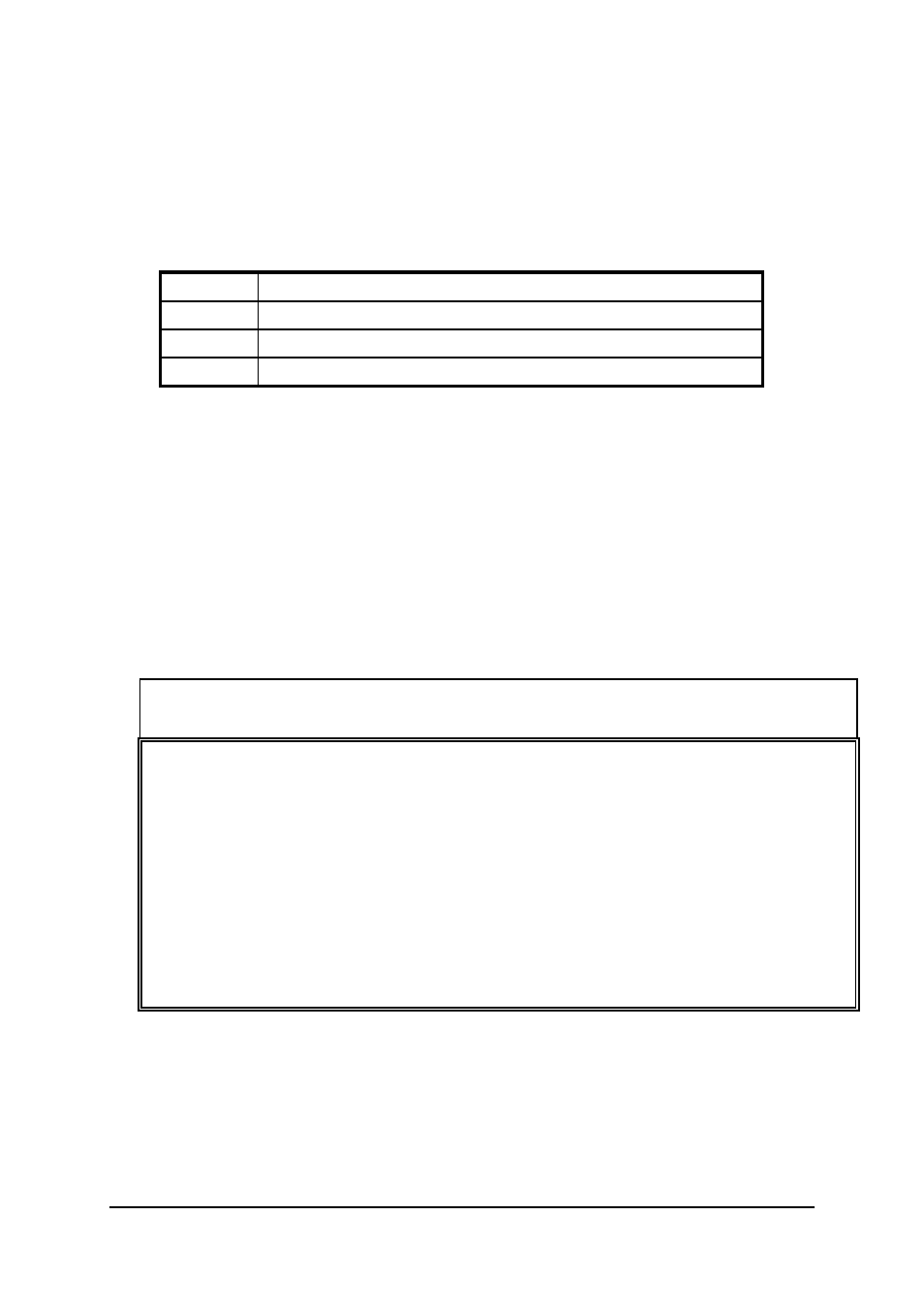
There are 4 variable resistors (VR) on the 9116 series board that allows you to
make adjustments to the A/D channels. The function of each VR is specified in
Table 18.
VR1
A/D unipolar offset adjustment
VR2
A/D bipolar offset adjustment
VR3
A/D full scale adjustment
VR4
PGA offset adjustment
Table 18. Functions of VRs
7.2.3 A/D
Adjustment
When you choose the calibration function from the main menu list, a calibration
items menu is displayed on the screen. After you have select one of the
calibration items from the calibration items menu, a calibration window displays
on the screen. The upper window outlines the
procedures that must be
carefully followed to calibrate the 9116 series card. The instructions will
guide you through the calibration process step by
step. The bottom
window shows the layout of the 9116 series card and the Variable Resister (VR)
that needs to be adjusted will blink.
****** cPCI-9116 Calibration ******
<1> A/D PGA offset adjusting
<2> A/D (Bipolar Gain = 1, -5V ~ 5V) adjusting
<3> A/D (Unipolar Gain = 1, 0V ~ 10V) adjusting
Select 1 to 3 or
Figure 23: A/D Adjustment menu Screen