7 a/d & fifo control register – ADLINK cPCI-9116 User Manual
Page 36
26
• Registers
4.7
A/D & FIFO Control Register
Address: BASE + 28
Attribute: Write
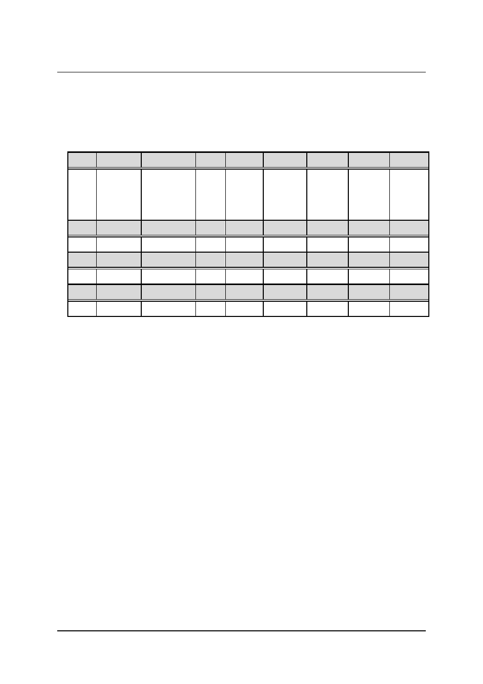
Data Format:
Bit
7
6
5
4
3
2
1
0
SC_dis
Clear
Channel
Gain
Queue
Set
done
Clear
DFIFO
Clear
Trg_det
Clear
SC_TC
Clear
ADOR
Clear
ADOS
Bit
15
14
13
12
11
10
9
8
--- --- ---
--- --- --- ---
DMA
Bit
23
22
21
20
19
18
17
16
--- --- ---
--- --- --- --- ---
Bit
31
30
29
28
27
26
25
24
--- --- ---
--- --- --- --- ---
Table 10. A/D & FIFO Control Register
DMA (Bit8): Write Only. Set for DMA transfer
SC_dis (Bit7): Write Only. Set to disable the SC counter
Clear Channel Gain Queue (Bit6): Write Only
Clear the Channel Gain Queue
0: no effect on the Channel Gain Queue
1: clear the Channel Gain Queue
Set done (Bit5): Write Only
0: indicate the Channel Gain Queue is not ready
1: indicate the Channel Gain Queue is OK
Clear DFIFO(Bit4) : Write Only
Clear the Data FIFO:
0: no effect on Data FIFO
1: clear the Data FIFO
Clear Trg_det(Bit3) : Write 1 to clear