2 internal timer/counter register – ADLINK cPCI-9116 User Manual
Page 31
Registers
• 21
4.2
Internal Timer/Counter Register
The 9116 series card basically has 6 counters, which are responsible for the
scan timing of the analog input data acquisition. The 6 counters occupy 6 I/O
address locations in the 9116 card as shown below.
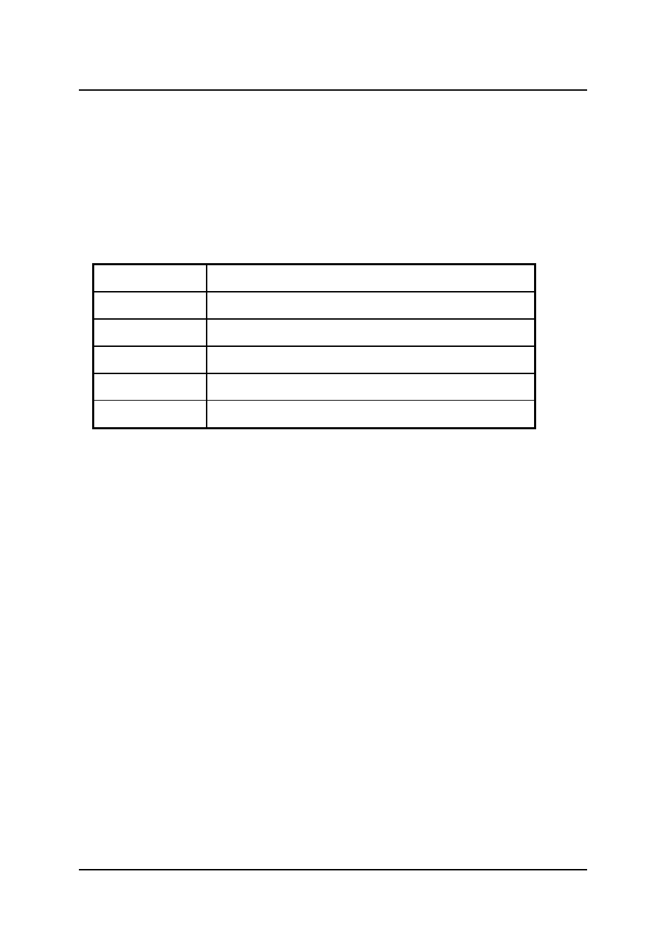
Address: BASE + 0 ~ BASE + 14
Attribute: read / write
Data Format:
Base + 0x00
Scan Interval Counter Register (R/W) 24bit
Base + 0x04
Sample Interval Counter Register (R/W) 16bit
Base + 0x08
Scan Counter Register (R/W) 24bit
Base + 0x0C
DIV Counter Register (R/W) 9bit
Base + 0x10
Delay1 Counter Register (R/W) 16bit
Base + 0x14
M Counter Register (R/W) 16bit
Table 3. Timer/Counter Register Address
SI_counter:
Scan Interval counter
SI2_counter:
Sample Interval counter
SC_counter:
total Scan Count counter
DIV_counter:
specify the number of samples per scan
DLY1_counter: Delay
Interval
counter (only used in delay trigger mode)
M_counter:
specify the number of scans before a trigger (only used in
pre-trigger and middle-trigger modes)