Solvline Eddy Series Ver 2.1a User Manual
Page 22
Chapter 3. Hardware
Description
3-7
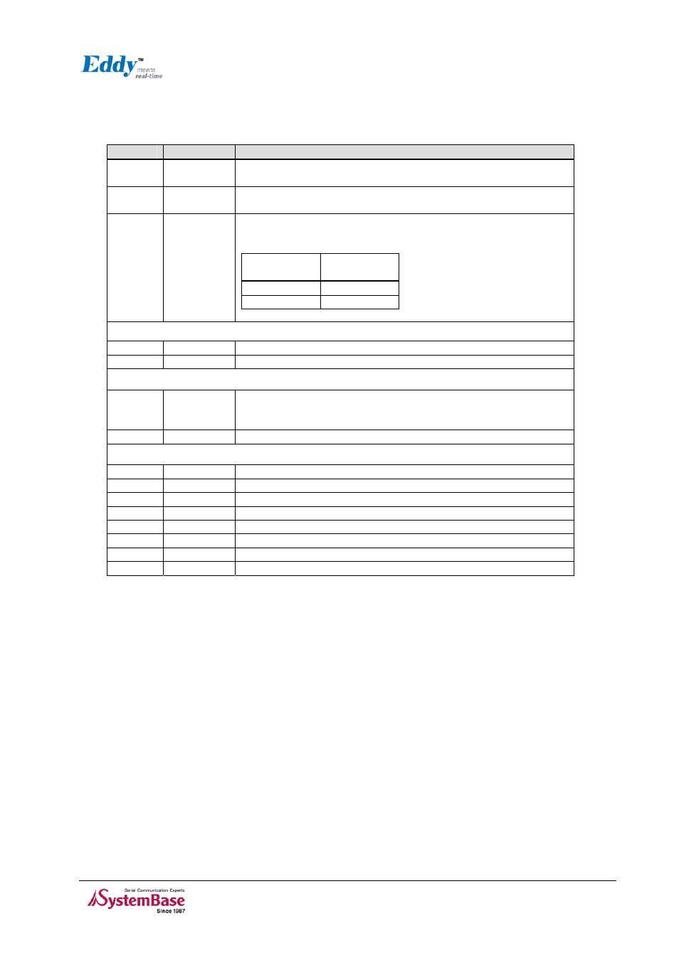
J3 Pin Description
Pin No
Name
Description
1-5 PID[4:0]
Product ID only used by the manufacturer.
Please do not work on these pins.
6, 25,
26
GND Ground
7~22 GPIO[1:16]
General Purpose In/Out signal
Development Kit’s LED adjustable
Pin State
LED
Definition
H ON
L OFF
Debug Unit - DBGU
23
DRXD
Debug Receive Data
24 DTXD
Debug
Transmit
Data
Reset/Test
27 BMS
Boot Mode Select signal
BMS = 1, Boot on Embedded ROM
BMS = 0, Boot on External Memory
28
NRST
External device Reset signal, active low signal
Universal Synchronous Asynchronous Receiver Transmitter USART0
29
DCD
USART0 Data Carrier Detection
30
RXD
USART0 Receive Data
31 TXD
USART0
Transmit
Data
32
DTR
USART0 Data Terminal Ready
33
DSR
USART0 Data Set Ready
34
RTS
USART0 Request To Send
35
CTS
USART0 Carrier To Send
36 RI
USART0
Ring
Indicator