Switching waveforms – Cypress Perform CY7C136A User Manual
Page 8
CY7C132, CY7C136
CY7C136A, CY7C142, CY7C146
Document #: 38-06031 Rev. *E
Page 8 of 15
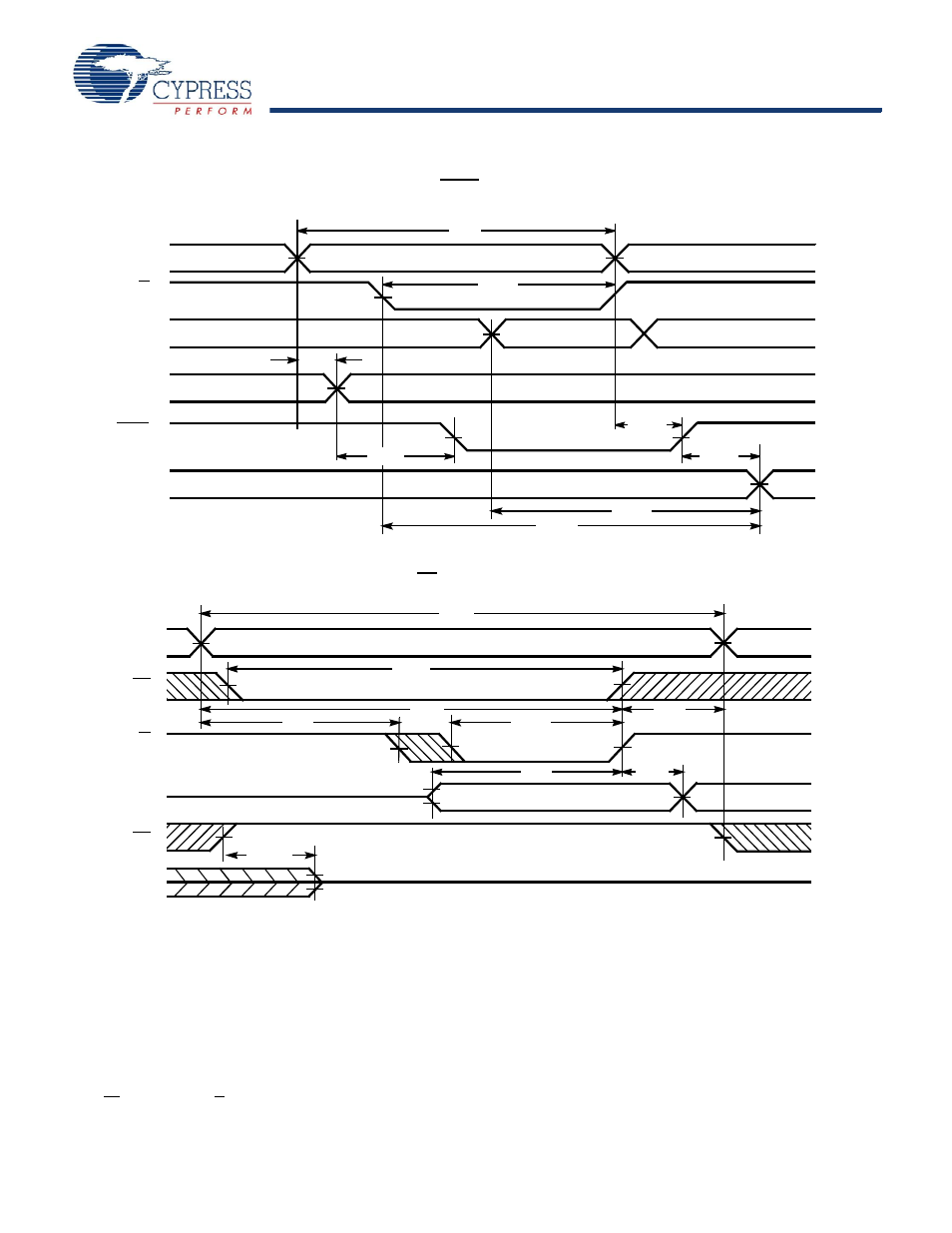
Figure 6. Read Cycle No. 3 (Read with BUSY Master: CY7C132 and CY7C136/CY7C136A)
Figure 7. Write Cycle No.1 (OE Three-States Data I/Os—Either Port)
Switching Waveforms
(continued)
t
BHA
t
BDD
VALID
t
DDD
t
WDD
ADDRESS MATCH
ADDRESS MATCH
R/W
R
ADDRESS
R
D
INR
ADDRESS
L
BUSY
L
DOUT
L
t
PS
t
BLA
t
RC
t
PWE
VALID
t
AW
t
WC
DATA VALID
HIGH IMPEDANCE
t
SCE
t
SA
t
PWE
t
HD
t
SD
t
HA
t
HZOE
CE
R/W
ADDRESS
OE
D
OUT
DATA
IN
Note
20. If OE is LOW during a R/W controlled write cycle, the write pulse width must be the larger of t
PWE
or t
HZWE
+ t
SD
to allow the data I/O pins to enter high impedance
and for data to be placed on the bus for the required t
SD
.
This manual is related to the following products: