Maximum ratings, Operating range, Electrical characteristics – Cypress Perform CY7C136A User Manual
Page 3
CY7C132, CY7C136
CY7C136A, CY7C142, CY7C146
Document #: 38-06031 Rev. *E
Page 3 of 15
Maximum Ratings
Exceeding maximum ratings may impair the useful life of the
device. These user guidelines are not tested.
Storage Temperature
..................................... −65°C to +150°C
Ambient Temperature with
Power Applied
.................................................. −55°C to +125°C
Supply Voltage to Ground Potential
(Pin 48 to Pin 24)
.................................................−0.5V to +7.0V
DC Voltage Applied to Outputs
in High Z State
.....................................................−0.5V to +7.0V
DC Input Voltage
.................................................−3.5V to +7.0V
Output Current into Outputs (LOW)............................. 20 mA
Static Discharge Voltage.......................................... > 2001V
(per MIL-STD-883, Method 3015)
Latch up Current.................................................... > 200 mA
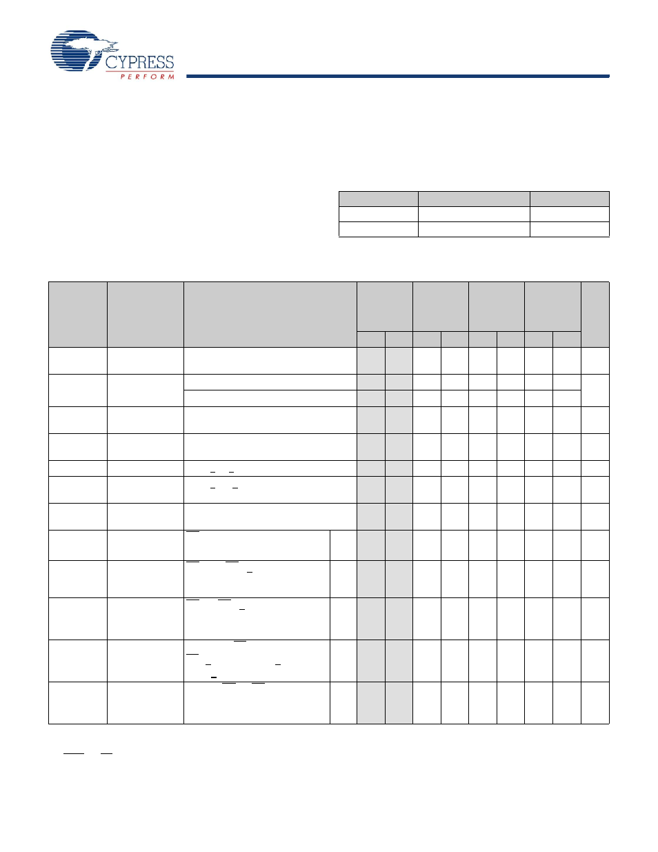
Operating Range
Range
Ambient Temperature
V
CC
Commercial
0°C to +70°C
5V ± 10%
Industrial
–40°C to +85°C
5V ± 10%
Notes
5. BUSY and INT pins only.
6. Duration of the short circuit should not exceed 30 seconds.
7. At f = f
MAX
, address and data inputs are cycling at the maximum frequency of read cycle of 1/t
rc
and using AC Test Waveforms input levels of GND to 3V.
Electrical Characteristics
Over the Operating Range
Parameter
Description
Test Conditions
7C136-15
[4]
7C146-15
7C132-30
[4]
7C136-25, 30
7C142-30
7C146-25, 30
7C132-35,45
7C136-35,45
7C142-35,45
7C146-35,45
7C132-55
7C136-55
7C136A-55
7C142-55
7C146-55
Unit
Min
Max
Min
Max
Min
Max
Min
Max
V
OH
Output HIGH
voltage
V
CC
= Min., I
OH
= –4.0 mA
2.4
2.4
2.4
2.4
V
V
OL
Output LOW
voltage
I
OL
= 4.0 mA
0.4
0.4
0.4
0.4
V
I
OL
= 16.0 mA
[5]
0.5
0.5
0.5
0.5
V
IH
Input HIGH
voltage
2.2
2.2
2.2
2.2
V
V
IL
Input LOW
voltage
0.8
0.8
0.8
0.8
V
I
IX
Input load current GND < V
I
< V
CC
–5
+5
−5
+5
−5
+5
−5
+5
μA
I
OZ
Output leakage
current
GND < V
O
< V
CC
, Output Disabled
–5
+5
−5
+5
−5
+5
−5
+5
μA
I
OS
Output short
circuit current
V
CC
= Max., V
OUT
= GND
–350
−350
−350
−350 mA
I
CC
V
CC
Operating
Supply Current
CE = V
IL
, Outputs Open,
f = f
MAX
Com’l/
Ind’l
190
170
120
110
mA
I
SB1
Standby current
both ports, TTL
Inputs
CE
L
and CE
R
> V
IH
,
f = f
MAX
Com’l/
Ind’l
75
65
45
35
mA
I
SB2
Standby Current
One Port,
TTL Inputs
CE
L
or CE
R
> V
IH
,
Active Port Outputs Open,
f = f
MAX
Com’l/
Ind’l
135
115
90
75
mA
I
SB3
Standby Current
Both Ports,
CMOS Inputs
Both Ports CE
L
and
CE
R
> V
CC
– 0.2V, V
IN
> V
CC
– 0.2V
or V
IN
< 0.2V, f = 0
Com’l/
Ind’l
15
15
15
15
mA
I
SB4
Standby Current
One Port,
CMOS Inputs
One Port CE
L
or CE
R
> V
CC
– 0.2V,
V
IN
> V
CC
– 0.2V or V
IN
< 0.2V,
Active Port Outputs Open, f = f
MAX
Com’l/
Ind’l
125
105
85
70
mA
Shaded areas contain preliminary information.