Digilent DIO1 User Manual
Page 2
Digilent DIO1 Reference Manual
Digilent, Inc.
www.digilentinc.com
page 2 of 10
Copyright Digilent, Inc. All rights reserved. Other product and company names mentioned may be trademarks of their respective owners.
signals arriving from an attached Digilab
system board are determined by the system
board, but all signals arising on the I/O board
derive from the on-board 5VDC regulator (so
they are all 5V CMOS signals).
The DIO1 board uses a two-layer process, so
all signals are available on the top and bottom
layers. Many signals are brought to a test point
header for easy test and measurement
equipment attachment.
Power Supply
The DIO1 board receives system power from
pins 39 and 37 of connectors A and B (which
mate to pins 1 and 3 of an attached system
boards). Pin 37 provides Vdd from the attached
system board (assumed to be 3.3VDC), and pin
39 is connected to ground. Up to 5VDC can be
safely applied to the Vdd input pin (pin 37).
The DIO1 board typically consumes less than
10mA with no LED’s illuminated, and up to
130mA with all LEDs illuminated (including
all segments of the seven-segment display).
Seven-segment LED display
The DIO1 board contains a modular 4-digit,
common anode, seven-segment LED display.
In a common anode display, the seven anodes
of the LEDs forming each digit are connected
to four common circuit nodes (labeled AN1
through AN4 on the DIO1 board). Each anode,
and therefore each digit, can be independently
turned on and off by driving these signals to a
‘1’ or a ‘0’. The cathodes of similar segments
on all four displays are also connected together
into seven common circuit nodes labeled CA
through CG. Thus, each cathode for all four
displays can be turned on and off
independently.
This connection scheme creates a multiplexed
display, where driving the anode signals and
corresponding cathode patterns of each digit in
a repeating, continuous succession can create a
4-digit display. In order for each of the four
digits to appear bright and continuously
illuminated, all four digits should be driven
once every 1 to 16ms (for a refresh frequency
of 60Hz to 1KHz). For example, in a 60Hz
refresh scheme, each digit would be illuminated
for ¼ of the refresh cycle, or 4ms. The
controller must assure that the correct cathode
pattern is present when the corresponding
anode signal is driven. To illustrate the process,
if AN1 is driven high while CB and CC are
driven low, then a “1” will be displayed in digit
position 2. Then, if AN2 is driven high while
CA, CB and CC are driven low, then a “7” will
be displayed in digit position 2. If AN1/CB, CC
are driven for 4ms, and then AN2/CA, CB, CC
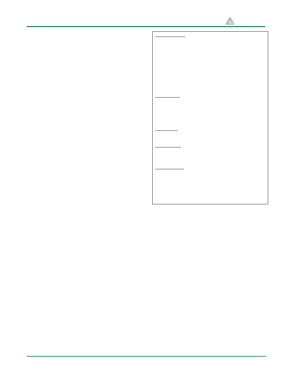
Power Supplies
VU
Unregulated power supply voltage from
attached system board – typically 5-
9VDC. Although connected to the board,
this supply is not used on the DIO1
board.
VDD33
Regulated power supply voltage
(3.3VDC) from attached system board.
All devices on DIO1 board use this
supply.
GND
System
ground
VGA signals
HS
VGA Horizontal Sync signal
VS
VGA Vertical Sync signal
R
VGA 1-bit red data
G
VGA 1-bit green data
B
VGA 1-bit blue data
PS2 signals
KCLK
PS2 (Keyboard or Mouse) clock signal
KDAT
PS2 (Keyboard or Mouse) data signal
Input devices
BTN1-4
Pushbuttons 1 through 4
SW1-
SW8
Slide switches 1 through 8
Output devices
LD0-LD8
Discreet LEDs 1 through 8
CA-CF
Seven-segment display cathodes
AN1-
AN3
Seven-segment display anodes
Table 1. DIO1 board signal definitions