Digilent DIO1 User Manual
Page 10
Digilent DIO1 Reference Manual
Digilent, Inc.
www.digilentinc.com
page 10 of 10
Copyright Digilent, Inc. All rights reserved. Other product and company names mentioned may be trademarks of their respective owners.
any given row. These two continually running
counters can be used to form an address into
video RAM. No time relationship between the
onset of the HS pulse and the onset of the VS
pulse is specified, so the designer can arrange
the counters to easily form video RAM
addresses, or to minimize decoding logic for
sync pulse generation.
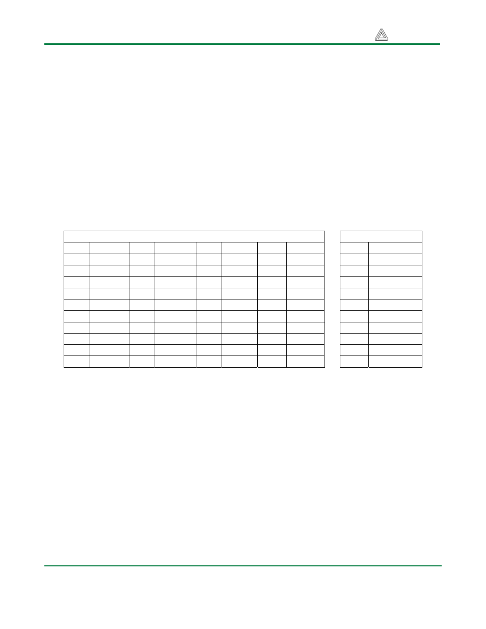
Connector pinouts
The connector pinouts are shown below.
Separately available tables show pass-through
connections for the devices on the DIO1 board
when the board is attached to various system
boards – i.e., one table is available showing the
FPGA connections to the DIO1 devices for a
D2 system board, another table is available
showing the FPGA connections for a D2E
board, a third for the D2XL board, etc.
J2 (B) connector
J1 (A) Connector
Pin Signal Pin Signal Pin Signal Pin Signal
Pin Signal
1 CA 11 CF 21 A1 31 n/c
30 BLU
2 SW1 12 SW6 22 LD1 32 LD6
32 PS2D
3 CB 13 CG 23
A2 33 n/c
33 GRN
4 SW2 14 SW7 24 LD2 34 LD7
34 PS2C
5 CC 15 DP 25
A3 35 n/c
35 RED
6 SW3 16 SW8 26 LD3 36 LD8
36 HS
7 CD 17
BTN2
27 A4 37
VDD33
37 VDD
8 SW4 18 BTN1 28 LD4 38 LDG
38 VS
9 CE 19
BTN4
29
n/c 39
GND
39 GND
10 SW5 20 BTN3 30 LD5 40 VU
40 VU