Gpio pins – Digilent 410-308P User Manual
Page 5
JTAG-SMT2-NC Reference Manual
Copyright Digilent, Inc. All rights reserved.
Other product and company names mentioned may be trademarks of their respective owners.
Page 5 of 14
In most cases, users can avoid a drive conflict by having applications that use the SMT2-NC communicate with the
TS in two-wire mode. Use the applications to reconfigure the TS to use the JScan0, JScan1, JScan2, or JScan3 scan
format prior to disabling the SMT2-NC’s JTAG port.
VIO
1149.7
Target
System
TDOC
TMSC
TDIC
TCKC
GND
VDD
VREF
TDO
JTAG-
SMT2-NC
GND
TMS
TDI
TCK
VIO
3.3V
VIO
200
VIO
1149.7
Target
System
TDOC
TMSC
TDIC
TCKC
GND
VDD
VREF
TDO
JTAG-
SMT2-NC
GND
TMS
TDI
TCK
VIO
3.3V
VIO
200
The Adept SDK provides an example application that demonstrates how to communicate with a Class T4 TAP
controller using the MScan, OScan0, and OScan1 scan formats.
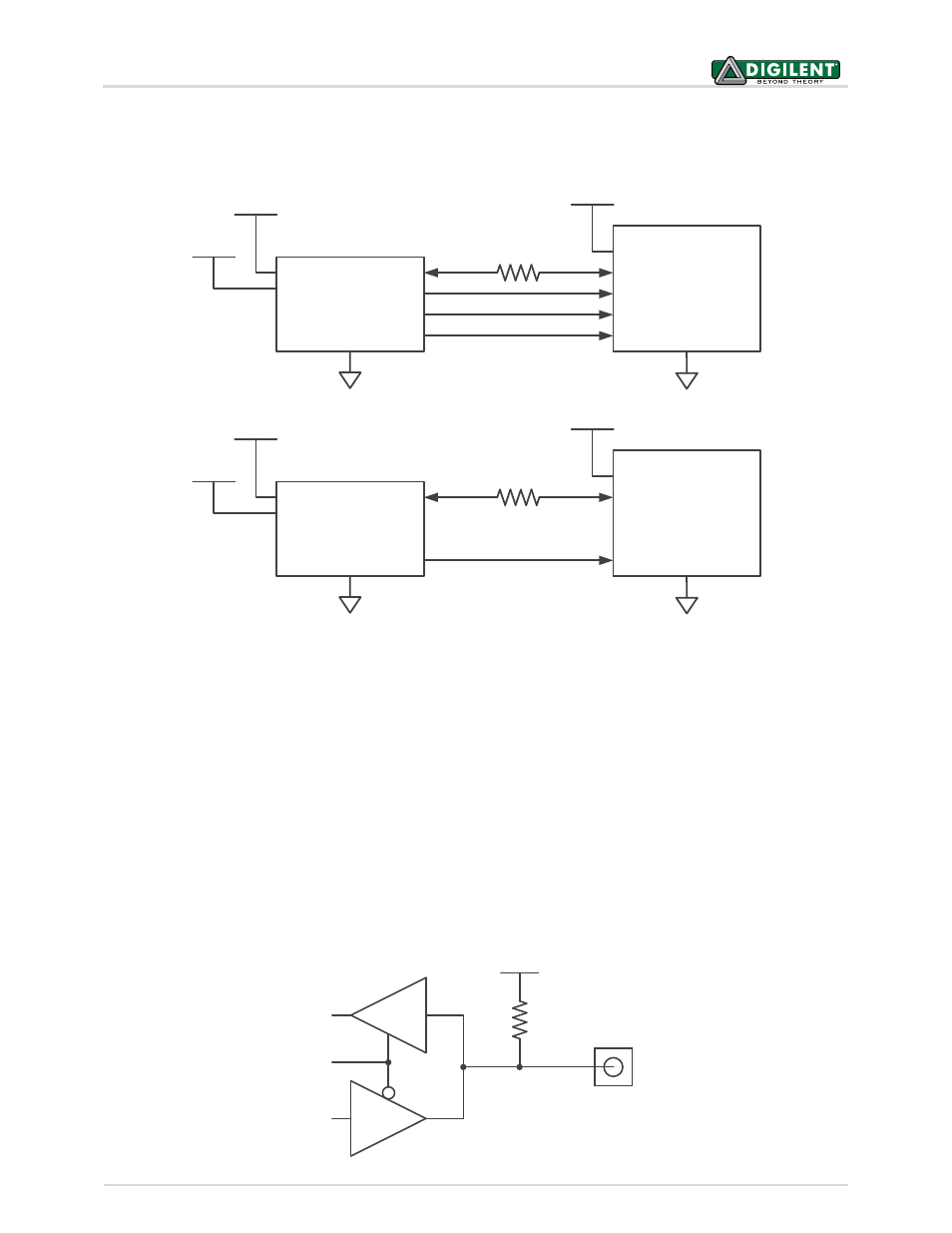
GPIO Pins
The JTAG-SMT2-NC has three general purpose I/O pins that are useful for a variety of different applications (GPIO0,
GPIO1, and GPIO2). Each pin features high speed three-state input and output buffers. At power up, the JTAG-
SMT2-NC disables these output buffers and places the signals in a high-impedance state. Each signal remains in a
high-impedance state until a host application enables DPIO port 0 and configures the applicable pin as an output.
When the host application disables DPIO port 0, all GPIO pins revert to a high-impedance state. Weak pull-ups
(100K ohm) ensure that the GPIO signals do not float while not being actively driven (see Fig. 8).
IO Pin
(GPIO0, GPIO1, GPIO2)
1
0
0
K
VREF
OEGPIOx
Figure 6. Adding a current limiting resistor.
Figure 7. 200 Ohm resistor limiting current flow.
Figure 8. GPIO signals.