Dc operating characteristics, Ac operating characteristics, Mounting to host pcbs – Digilent 210-251P-BOARD User Manual
Page 10
JTAG-SMT2 Reference Manual
Copyright Digilent, Inc. All rights reserved.
Other product and company names mentioned may be trademarks of their respective owners.
Page 10 of 11
DC Operating Characteristics
Symbol
Parameter
Min
Typ
Max
Unit
Vdd
Operating supply voltage
2.97
3.3
3.63
Volts
Vref
I/O reference/supply voltage
1.65
2.5/3.3
5.5
Volts
TDO, GPIO0,
GPIO1, GPIO2
Input High Voltage (V
IH
)
1.62
5.5
Volts
Input Low Voltage (V
IL
)
0
0.65
Volts
TMS, TCK, TDI,
GPIO0, GPIO1,
GPIO2
Output High (V
OH
)
0.85 x Vref
0.95 x Vref
Vref
Volts
Output Low (V
OL
)
0
0.05 x Vref
0.15 x Vref
Volts
T
A
Operating Temperature
0
70
ºC
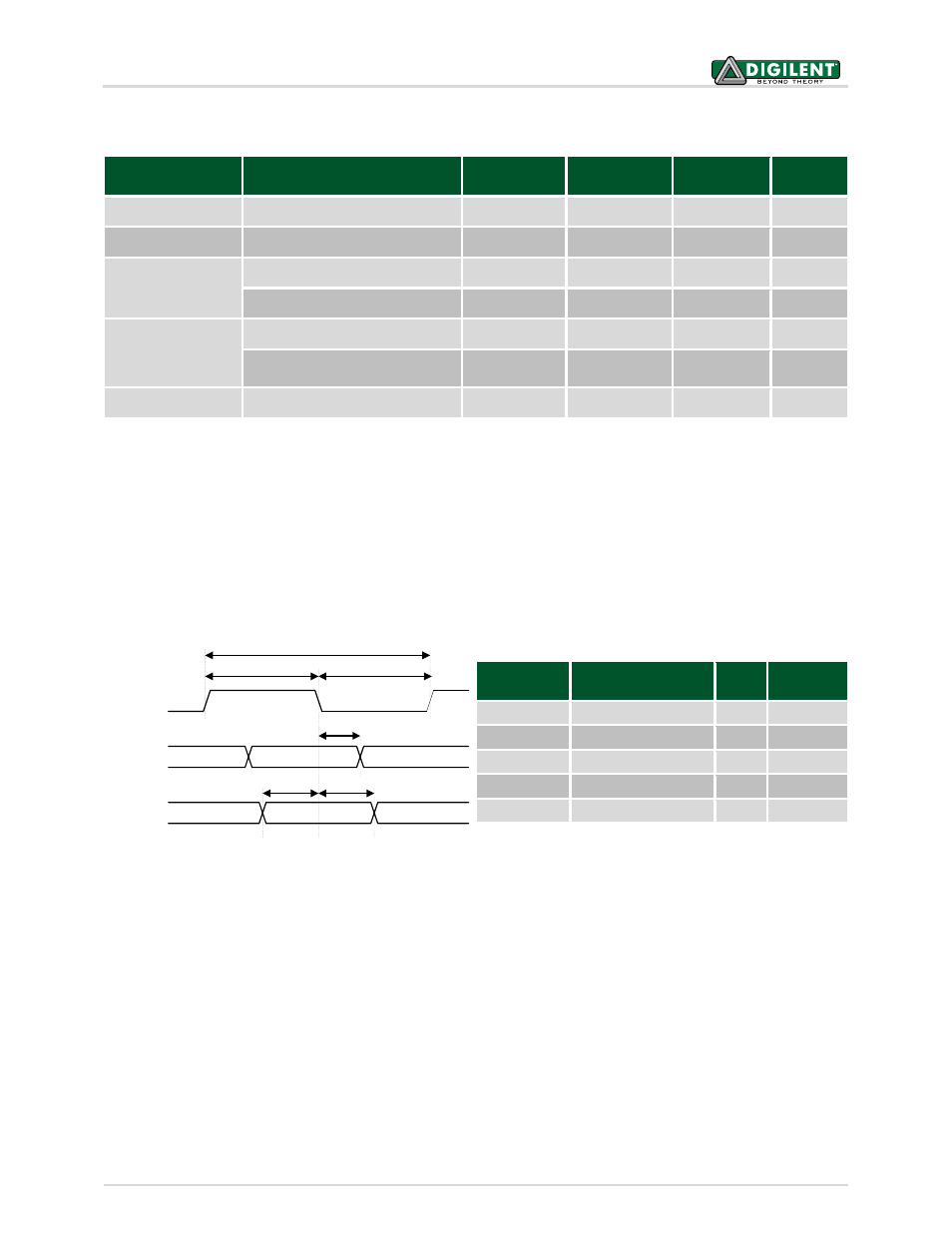
AC Operating Characteristics
The JTAG-SMT2’s JTAG signals operate according to the timing diagram in Fig. 12. The SMT2 supports JTAG/TCK
frequencies from 30 MHz to 8 KHz at integer divisions of 30 MHz from 1 to 3750. Common frequencies include 30
MHz, 15 MHz, 10 Mhz, 7.5 MHz, and 6 MHz (see Table 2). The JTAG/TCK operating frequency can be set within the
Xilinx Tools. Note: Please refer to Xilinx’s iMPACT documentation for more information.
Symbol
Parameter
Min
Max
T
CK
T
CK
period
33ns
2.185ms
T
CKH
, T
CKL
T
CLK
pulse width
20ns
1.1ms
T
CD
T
CLK
to TMS, TDI
0
15ns
T
SU
TDO Setup time
19ns
T
HD
TDO Hold time
0
Mounting to Host PCBs
The JTAG-SMT2 module has a moisture sensitivity level (MSL) of 6. Prior to reflow, the JTAG-SMT2 module must be
dried by baking it at 125° C for 17 hours. Once this process has been completed, the module has a MSL of 3 and is
suitable for reflow for up to 168 hours without additional drying.
The factory finishes the JTAG-SMT2 signal pads with the ENIG process using 2u” gold over 150u” electroless nickel.
This makes the SMT2 compatible with most mounting and reflow processes (see Fig. 13). The binding force of the
solder is sufficient to hold the SMT2 firmly in place so mounting should require no additional adhesives.
Figure 12. Timing diagram.
TMS/TDI
TCK
TDO
T
CKL
T
CKH
T
CK
T
CD
T
SU
T
HD
Table 2. JTAG frequency support.