Digilent 210-251P-BOARD User Manual
Jtag-smt2 programming module for xilinx, Fpgas, Overview
1300 Henley Court
Pullman, WA 99163
509.334.6306
www.digilentinc.com
JTAG-SMT2
Programming Module for Xilinx
®
FPGAs
Revised March 2, 2015
DOC#: 502-251
Copyright Digilent, Inc. All rights reserved.
Other product and company names mentioned may be trademarks of their respective owners.
Page 1 of 11
Overview
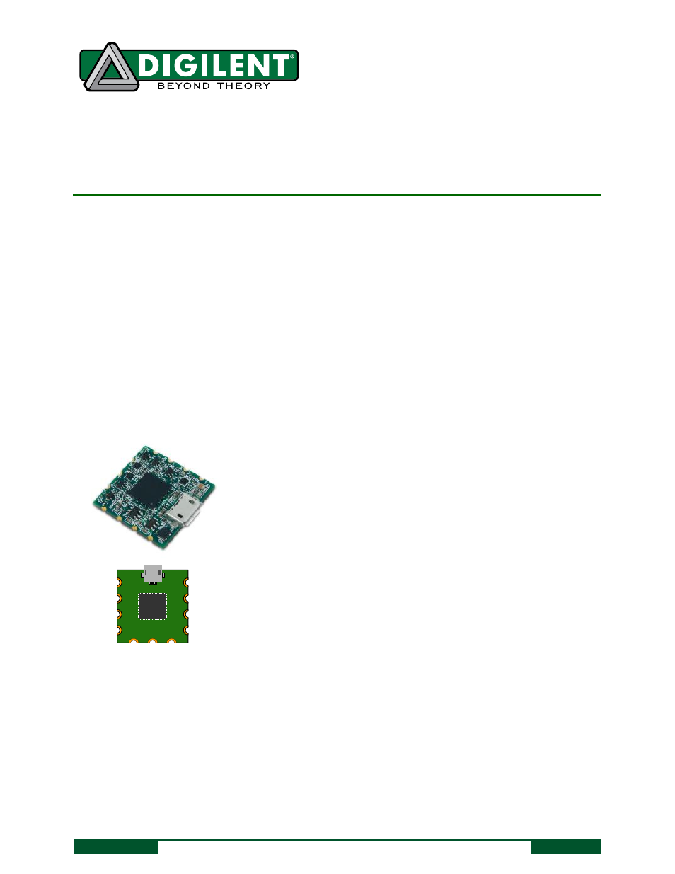
The Joint Test Action Group (JTAG)-SMT2 is a compact, complete and fully self-contained surface-mount
programming module for Xilinx field-programmable gate arrays (FPGAs). The module can be accessed directly from
all Xilinx Tools, including iMPACT, Chipscope™, and EDK. Users can load the module directly onto a target board
and reflow it like any other component.
The JTAG-SMT2 uses a 3.3V main power supply and a separate Vref supply to drive the JTAG signals. All JTAG
signals use high speed, 24mA, three-state buffers that allow signal voltages from 1.8V to 5V and bus speeds of up
to 30MBit/sec. The JTAG bus can be shared with other devices as systems hold JTAG signals at high-impedance,
except when actively driven during programming. The SMT2 module is CE certified and fully compliant with EU
RoHS and REACH directives. The module uses a standard Type-A to Micro-USB cable available for purchase from
Digilent, Inc.
Users can connect JTAG signals directly to the corresponding FPGA signals, as shown in Fig. 1. For best results,
mount the module adjacent to the edge of the host PCB over a ground plane. Although users may run signal traces
on top of the host PCB beneath the SMT2, Digilent recommends keeping the area immediately beneath the SMT2
clear.
Note: Keep the impedance between the SMT2 and FPGA below 100 Ohms to operate the JTAG at maximum speed.
1
2
3
4
8
9
10
11
5
6
7
GND
TCK
TDI
TMS
G
P
IO
1
G
P
IO
2
G
P
IO
0
TDO
VREF
GND
Vdd (3.3V)
Small, complete, all-in-one JTAG programming/debugging
solution for Xilinx FPGAs
Compatible with all Xilinx Tools
Compatible with IEEE 1149.7-2009 Class T0 – Class T4
(includes 2-Wire JTAG)
GPIO pin allows debugging software to reset the processor
core of Xilinx’s Zynq® platform
Single 3.3V supply
Separate Vref drives JTAG signal voltages; Vref can be any
voltage between 1.8V and 5V.
High-Speed USB2 port that can drive JTAG/SPI bus at up to
30Mbit/sec (frequency settable by user)
SPI programming solution (modes 0 and 2 up to 30Mbit/sec,
modes 1 and 3 up to 2Mbit/sec)
Uses micro-AB USB2 connector
Small form-factor surface-mount module can be directly
loaded on target boards
A similar circuit is available as a stand-alone programming
cable; see Digilent’s JTAG-HS2.
Features include:
The JTAG-SMT2