14 digital i/o interface, 1 multifunction overview, Ktt20/pitx user's guide – Kontron KTT20-pITX User Manual
Page 31
KTD-S0044-G
Page 27
Digital I/O Interface
KTT20/pITX User's Guide
14 Digital I/O Interface
The digital I/O interface is a subset of a multifunction part from NVIDIAs
®
Tegra
®
250 SoC. Most of the I/O
pins have additional functionalities which can be changed by software using two I/O connectors with
different signal voltages.
14.1 Multifunction Overview
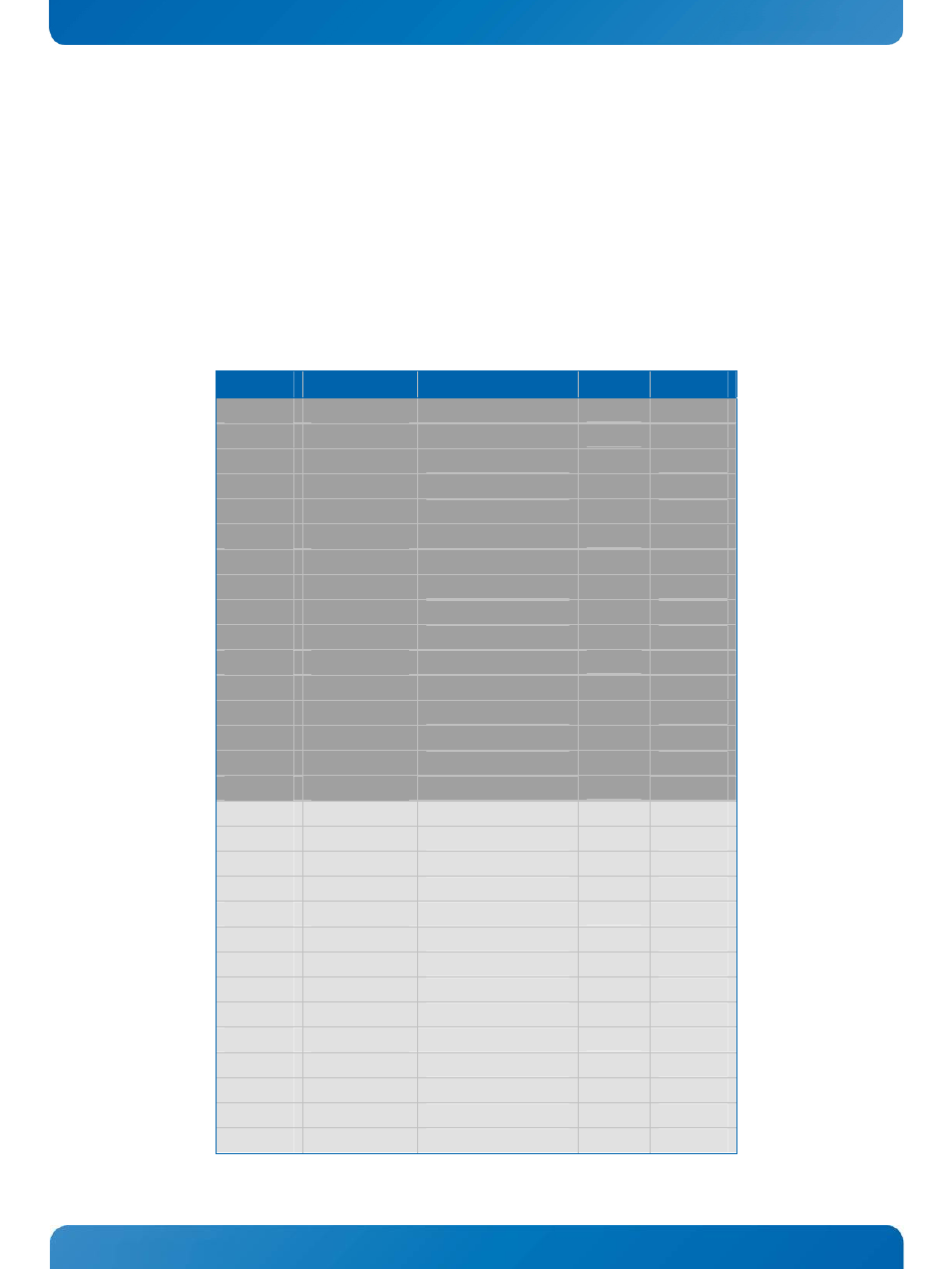
The following table informs about the dependencies.
I/O Pin
NVIDIA
®
Label
Second Function
Voltage Connector
GPIO0
R.05
Keyboard row 5
1.8V
J1300
GPIO1
R.06
Keyboard row 6
1.8V
J1300
GPIO2
R.07
Keyboard row 7
1.8V
J1300
GPIO3
S.00
Keyboard row 8
1.8V
J1300
GPIO4
S.01
Keyboard row 9
1.8V
J1300
GPIO5
S.02
Keyboard row 10
1.8V
J1300
GPIO6
S.04
Keyboard row 12
1.8V
J1300
GPIO7
S.05
Keyboard row 13
1.8V
J1300
GPIO8
Q.00
Keyboard column 0
1.8V
J1300
GPIO9
Q.01
Keyboard column 1
1.8V
J1300
GPIO10
Q.02
Keyboard column 2
1.8V
J1300
GPIO11
Q.03
Keyboard column 3
1.8V
J1300
GPIO12
Q.04
Keyboard column 4
1.8V
J1300
GPIO13
Q.05
Keyboard column 5
1.8V
J1300
GPIO14
Q.06
Keyboard column 6
1.8V
J1300
GPIO15
Q.07
Keyboard column 7
1.8V
J1300
GPIO16
B.02
I
2
C
TM
clock
3.3V
J2001
GPIO17
B.03
I
2
C
TM
data
3.3V
J2001
GPIO18
T.02
SPI1
TM
MOSI
3.3V
J2001
GPIO19
T.03
SPI1
TM
MISO
3.3V
J2001
GPIO20
B.04
SPI1
TM
clock
3.3V
J2001
GPIO21
B.05
SPI1
TM
chip select
3.3V
J2001
GPIO22
T.04
---------
3.3V
J2001
GPIO23
D.05
SDIO2 command line
3.3V
J2001
GPIO24
L.00
SDIO2 data 0
3.3V
J2001
GPIO25
L.01
SDIO2 data 1
3.3V
J2001
GPIO26
L.02
SDIO2 data 2
3.3V
J2001
GPIO27
L.03
SDIO2 data 3
3.3V
J2001
GPIO28
L.04
SDIO2 data 4
3.3V
J2001
GPIO29
L.05
SDIO2 data 5
3.3V
J2001