2 adc control logic, Adc control logic - 8, Adc common control register bit map - 8 – Kontron CP371 User Manual
Page 52: Rng, bip bits - 8, Adc data registers bit map - 8, Configuration cp371
Configuration
CP371
Page 4 - 8
© 2002 PEP Modular Computers GmbH
ID 23762, Rev. 02
4.3.2
ADC Control Logic
This part of the IO Control Logic controls the communication with the ADC (MAX1270). The
ADC integrates 8 channels per chip ( 2 clusters for a total of 16 channels) and has a serial bus
interface operating at 2 MHz.
ADC operating mode is individually programmable for each channel, i.e. the polarity (unipo-
lar/bipolar) and range (5/10/20V). After initialization of the corresponding ADC Control Regis-
ters an Enable Bit must be set to ‘1’.
The ADC Control Logic handles the cyclic setup of the necessary ADC control word including
start bit, channel address, channel mode, and clock mode without any software intervention.
The digitized data are automatically stored in dual-ported data registers. An arbiter avoids ac-
cess conflicts between PCI access and ADC access to the same data register.
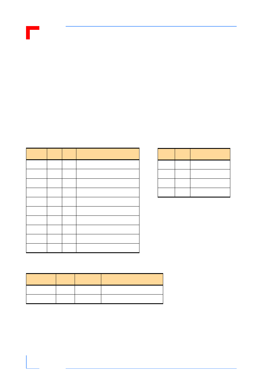
Table 4-2: ADC Common Control Register
Bit Map
BITS
TYP. DEF.
FUNCTION
31
R/W
0
Enable
30 - 16
R/W
00
reserved
15 - 14
R/W
00
RNG, BIP for ADC channel # 7
13 - 12
R/W
00
RNG, BIP for ADC channel # 6
11 - 10
R/W
00
RNG, BIP for ADC channel # 5
9 - 8
R/W
00
RNG, BIP for ADC channel # 4
7 - 6
R/W
00
RNG, BIP for ADC channel # 3
5 - 4
R/W
00
RNG, BIP for ADC channel # 2
3 - 2
R/W
00
RNG, BIP for ADC channel # 1
1 - 0
R/W
00
RNG, BIP for ADC channel # 0
Table 4-4: ADC Data Registers Bit Map
BITS
TYPE
DEFAULT
FUNCTION
31 - 12
R
0
reserved
11 - 0
R
0
Data, 12 bit digit
Table 4-3: RNG, BIP Bits
RNG
BIP
INPUT RANGE
0
0
0 – 5 V
1
0
0 – 10 V
0
1
– 5 V
1
1
– 10 V