Package diagrams – Cypress CY7C1380C User Manual
Page 33

CY7C1380C
CY7C1382C
Document #: 38-05237 Rev. *D
Page 33 of 36
© Cypress Semiconductor Corporation, 2004. The information contained herein is subject to change without notice. Cypress Semiconductor Corporation assumes no responsibility for the use
of any circuitry other than circuitry embodied in a Cypress Semiconductor product. Nor does it convey or imply any license under patent or other rights. Cypress Semiconductor does not authorize
its products for use as critical components in life-support systems where a malfunction or failure may reasonably be expected to result in significant injury to the user. The inclusion of Cypress
Semiconductor products in life-support systems application implies that the manufacturer assumes all risk of such use and in doing so indemnifies Cypress Semiconductor against all charges.
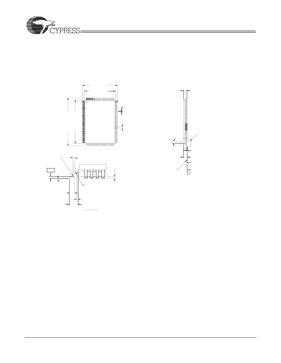
Package Diagrams
DIMENSIONS ARE IN MILLIMETERS.
0.30±0.08
0.65
20.00±0.10
22.00±0.20
1.40±0.05
12°±1°
1.60 MAX.
0.05 MIN.
0.60±0.15
0° MIN.
0.25
0°-7°
(8X)
STAND-OFF
R 0.08 MIN.
TYP.
0.20 MAX.
0.15 MAX.
0.20 MAX.
R 0.08 MIN.
0.20 MAX.
14.00±0.10
16.00±0.20
0.10
SEE DETAIL
A
DETAIL
A
1
100
30
31
50
51
80
81
GAUGE PLANE
1.00 REF.
0.20 MIN.
SEATING PLANE
100-Pin Thin Plastic Quad Flatpack (14 x 20 x 1.4 mm) A101
51-85050-*A
