Cypress CY7C1380C User Manual
Page 19
CY7C1380C
CY7C1382C
Document #: 38-05237 Rev. *D
Page 19 of 36
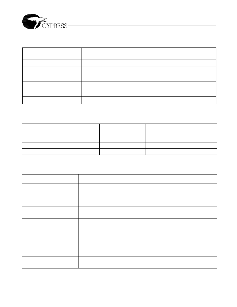
Identification Register Definitions
INSTRUCTION FIELD
CY7C1380C
(512KX36)
CY7C1382C
(1MX18)
DESCRIPTION
Revision Number (31:29)
010
0100
Describes the version number.
Device Depth (28:24)
01010
1010
Reserved for Internal Use
Device Width (23:18)
000000
000000
Defines memory type and architecture
Cypress Device ID (17:12)
100101
010101
Defines width and density
Cypress JEDEC ID Code (11:1)
00000110100
00000110100
Allows unique identification of SRAM vendor.
ID Register Presence Indicator (0)
1
1
Indicates the presence of an ID register.
Scan Register Sizes
REGISTER NAME
BIT SIZE(X36)
BIT SIZE(X18)
Instruction
3
3
Bypass
1
1
ID
32
32
Boundary Scan Order
72
72
Identification Codes
INSTRUCTION
CODE
DESCRIPTION
EXTEST
000
Captures I/O ring contents. Places the boundary scan register between TDI and TDO.
Forces all SRAM outputs to High-Z state. This instruction is not 1149.1 compliant.
IDCODE
001
Loads the ID register with the vendor ID code and places the register between TDI and
TDO. This operation does not affect SRAM operations.
SAMPLE Z
010
Captures I/O ring contents. Places the boundary scan register between TDI and TDO.
Forces all SRAM output drivers to a High-Z state.
RESERVED
011
Do Not Use: This instruction is reserved for future use.
SAMPLE/PRELOAD
100
Captures I/O ring contents. Places the boundary scan register between TDI and TDO.
Does not affect SRAM operation. This instruction does not implement 1149.1 preload
function and is therefore not 1149.1 compliant.
RESERVED
101
Do Not Use: This instruction is reserved for future use.
RESERVED
110
Do Not Use: This instruction is reserved for future use.
BYPASS
111
Places the bypass register between TDI and TDO. This operation does not affect
SRAM operations.