Cypress CY7C1380C User Manual
Page 17
CY7C1380C
CY7C1382C
Document #: 38-05237 Rev. *D
Page 17 of 36
Note that since the PRELOAD part of the command is not
implemented, putting the TAP to the Update-DR state while
performing a SAMPLE/PRELOAD instruction will have the
same effect as the Pause-DR command.
BYPASS
When the BYPASS instruction is loaded in the instruction
register and the TAP is placed in a Shift-DR state, the bypass
register is placed between the TDI and TDO balls. The
advantage of the BYPASS instruction is that it shortens the
boundary scan path when multiple devices are connected
together on a board.
Reserved
These instructions are not implemented but are reserved for
future use. Do not use these instructions.
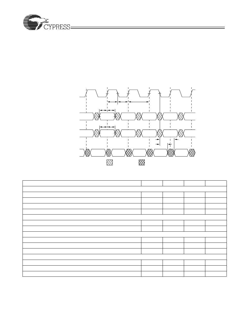
TAP Timing
TAP AC Switching Characteristics Over the operating Range
Parameter
Symbol
Min
Max
Units
Clock
TCK Clock Cycle Time
t
TCYC
100
ns
TCK Clock Frequency
t
TF
10
MHz
TCK Clock HIGH time
t
TH
40
ns
TCK Clock LOW time
t
TL
40
ns
Output Times
TCK Clock LOW to TDO Valid
t
TDOV
20
ns
TCK Clock LOW to TDO Invalid
t
TDOX
0
ns
Setup Times
TMS Set-Up to TCK Clock Rise
t
TMSS
10
ns
TDI Set-Up to TCK Clock Rise
t
TDIS
10
ns
Capture Set-Up to TCK Rise
t
CS
10
Hold Times
TMS hold after TCK Clock Rise
t
TMSH
10
ns
TDI Hold after Clock Rise
t
TDIH
10
ns
Capture Hold after Clock Rise
t
CH
10
ns
Notes:
9.
t
CS and
t
CH refer to the setup and hold time requirements of latching data from the boundary scan register.
10. Test conditions are specified using the load in TAP AC test Conditions. t
R
/t
F
= 1ns.
t
TL
Test Clock
(TCK)
1
2
3
4
5
6
Test Mode Select
(TMS)
tTH
Test Data-Out
(TDO)
tCYC
Test Data-In
(TDI)
tTMSH
tTMSS
tTDIH
tTDIS
tTDOX
tTDOV
DON’T CARE
UNDEFINED