Thermal resistance, Capacitance, Electrical characteristics – Cypress CY7C1380C User Manual
Page 25
CY7C1380C
CY7C1382C
Document #: 38-05237 Rev. *D
Page 25 of 36
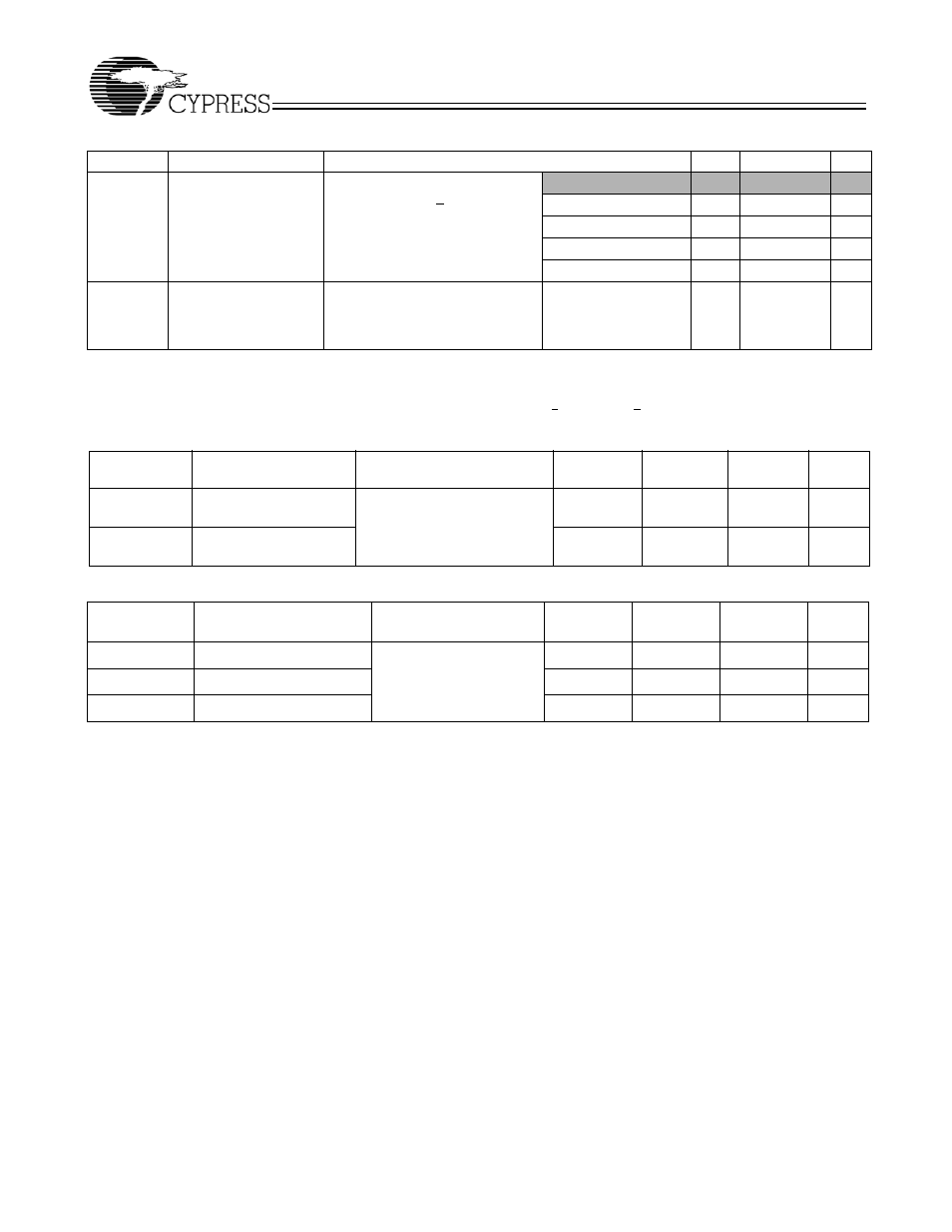
I
SB3
Automatic CE
Power-down
Current—CMOS Inputs
V
DD
= Max, Device Deselected, or
V
IN
≤ 0.3V or V
IN
> V
DDQ
– 0.3V
f = f
MAX
= 1/t
CYC
4.0-ns cycle, 250 MHz
105
mA
4.4-ns cycle, 225 MHz
100
mA
5.0-ns cycle, 200 MHz
95
mA
6.0-ns cycle, 167 MHz
85
mA
7.5-ns cycle, 133 MHz
80
mA
I
SB4
Automatic CE
Power-down
Current—TTL Inputs
V
DD
= Max, Device Deselected,
V
IN
≥ V
IH
or V
IN
≤ V
IL
, f = 0
All speeds
80
mA
Shaded areas contain advance information.
Notes:
12. Overshoot: V
IH
(AC) < V
DD
+1.5V (Pulse width less than t
CYC
/2), undershoot: V
IL
(AC) > -2V (Pulse width less than t
CYC
/2).
13. TPower-up: Assumes a linear ramp from 0v to V
DD
(min.) within 200ms. During this time V
IH
< V
DD
and V
DDQ
< V
DD\
Thermal Resistance
Parameter
Description
Test Conditions
TQFP
Package
BGA
Package
fBGA
Package
Unit
Θ
JA
Thermal Resistance
(Junction to Ambient)
Test conditions follow standard
test methods and procedures
for measuring thermal
impedence, per EIA / JESD51.
31
45
46
°C/W
Θ
JC
Thermal Resistance
(Junction to Case)
6
7
3
°C/W
Capacitance
Parameter
Description
Test Conditions
TQFP
Package
BGA
Package
fBGA
Package
Unit
C
IN
Input Capacitance
T
A
= 25
°C, f = 1 MHz,
V
DD
= 3.3V.
V
DDQ
= 2.5V
5
8
9
pF
C
CLK
Clock Input Capacitance
5
8
9
pF
C
I/O
Input/Output Capacitance
5
8
9
pF
Notes:
14. Tested initially and after any design or process change that may affect these parameters
Electrical Characteristics
Over the Operating Range
[12, 13] (continued)
Parameter
Description
Test Conditions
Min.
Max.
Unit