Switching waveforms, Read/write/deselect sequence, Switching waveforms read/write/deselect sequence – Cypress CY7C1165V18 User Manual
Page 25
CY7C1161V18, CY7C1176V18
CY7C1163V18, CY7C1165V18
Document Number: 001-06582 Rev. *D
Page 25 of 29
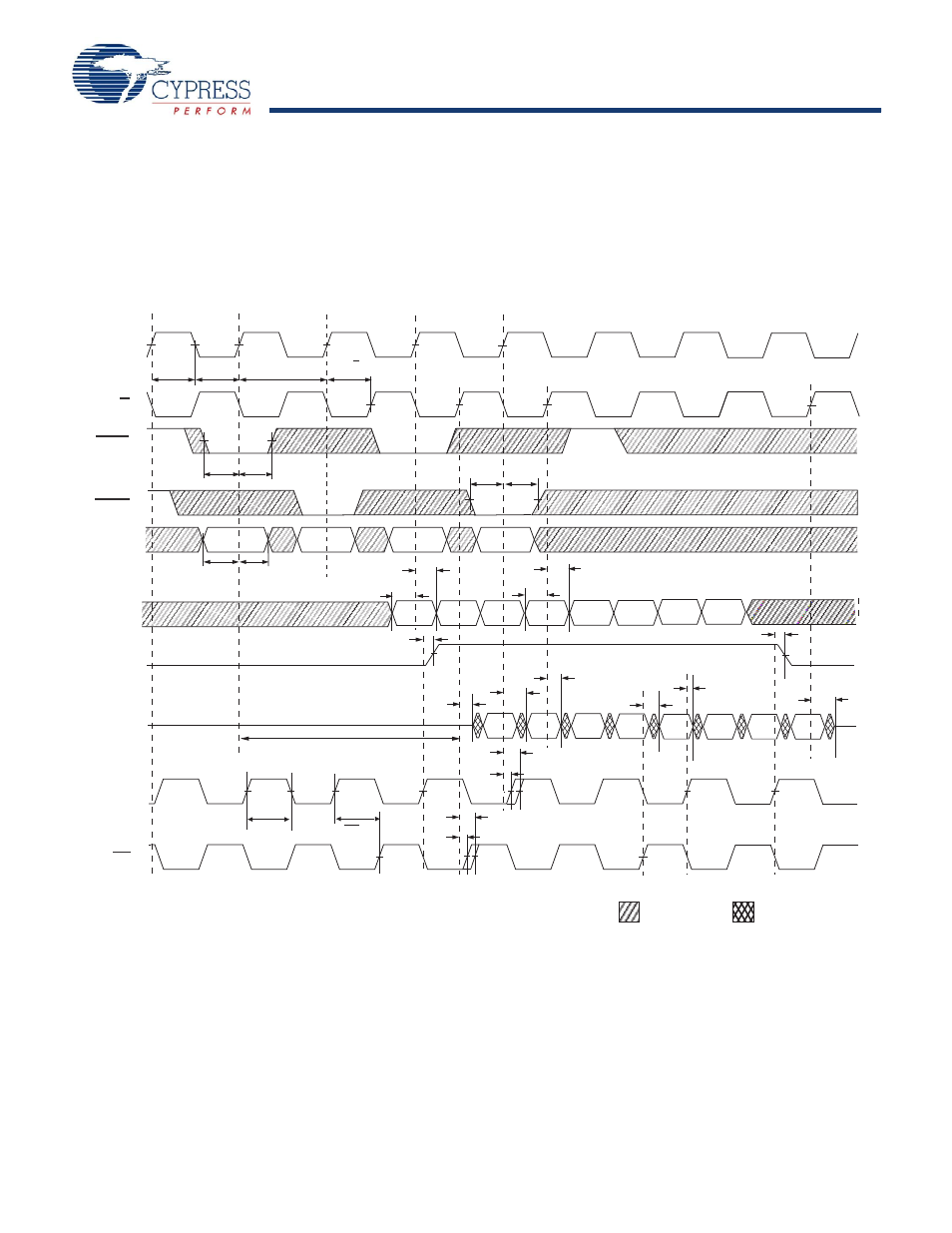
Switching Waveforms
Read/Write/Deselect Sequence
Figure 6. Waveform for 2.5 Cycle Read Latency
tKH
tKL
tCYC
tKHKH
t
t
t
tSA
HA
SC
HC
tHD
tSC tHC
A0
A1
A2
A3
t
t
SD
HD
t SD
D11
D10
D12
D13
D30
D31
D32
D33
D
A
WPS
RPS
K
K
t
NOP
READ
NOP
WRITE
READ
WRITE
1
2
3
4
5
6
7
8
CQ
CQ
Q
tCQOH
CCQO
t
CLZ
t
t
CO
tDOH
tCQDOH
CQD
t
tCHZ
tCQOH
CCQO
t
tQVLD
QVLD
QVLD
DON’T CARE
UNDEFINED
(Read Latency = 2.5 Cycles)
Q00
Q01
Q20
Q02
Q21
Q03
Q22
Q23
tCQH
t
CQHCQH
Notes
31. Q00 refers to output from address A0. Q01 refers to output from the next internal burst address following A0, i.e., A0+1.
32. Outputs are disabled (High Z) one clock cycle after a NOP.
33. In this example, if address A2 = A1, then data Q20 = D10 and Q21 = D11. Write data is forwarded immediately as read results. This note applies to the whole diagram.