Ac electrical characteristics, Capacitance, Thermal resistance – Cypress Perform CY7C1561V18 User Manual
Page 22
CY7C1561V18, CY7C1576V18
CY7C1563V18, CY7C1565V18
Document Number: 001-05384 Rev. *F
Page 22 of 28
AC Electrical Characteristics
Over the Operating Range
Parameter
Description
Test Conditions
Min
Typ
Max
Unit
V
IH
Input HIGH Voltage
V
REF
+ 0.2
–
V
DDQ
+ 0.24
V
V
IL
Input LOW Voltage
–0.24
–
V
REF
– 0.2
V
Capacitance
Tested initially and after any design or process change that may affect these parameters.
Parameter
Description
Test Conditions
Max
Unit
C
IN
Input
Capacitance
T
A
= 25
°C, f = 1 MHz, V
DD
= 1.8V, V
DDQ
= 1.5V
5
pF
C
CLK
Clock Input Capacitance
6
pF
C
O
Output Capacitance
7
pF
Thermal Resistance
Tested initially and after any design or process change that may affect these parameters.
Parameter
Description
Test Conditions
165 FBGA
Package
Unit
Θ
JA
Thermal Resistance
(Junction to Ambient)
Test conditions follow standard test methods and
procedures for measuring thermal impedance, in
accordance with EIA/JESD51.
11.82
°C/W
Θ
JC
Thermal Resistance
(Junction to Case)
2.33
°C/W
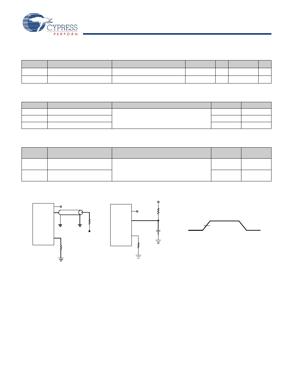
Figure 4. AC Test Loads and Waveforms
1.25V
0.25V
R = 50
Ω
5 pF
INCLUDING
JIG AND
SCOPE
ALL INPUT PULSES
Device
R
L
= 50
Ω
Z
0
= 50
Ω
V
REF
= 0.75V
V
REF
= 0.75V
0.75V
Under
Test
0.75V
Device
Under
Test
OUTPUT
0.75V
V
REF
V
REF
OUTPUT
ZQ
ZQ
(a)
Slew Rate = 2 V/ns
RQ =
250
Ω
(b)
RQ =
250
Ω
Notes
23. Unless otherwise noted, test conditions assume signal transition time of 2V/ns, timing reference levels of 0.75V, Vref = 0.75V, RQ = 250
Ω, V
DDQ
= 1.5V, input pulse
levels of 0.25V to 1.25V, and output loading of the specified I
OL
/I
OH
and load capacitance shown in (a) of