Cypress CY7C1360C User Manual
Page 31
CY7C1360C
CY7C1362C
Document #: 38-05540 Rev. *H
Page 31 of 31
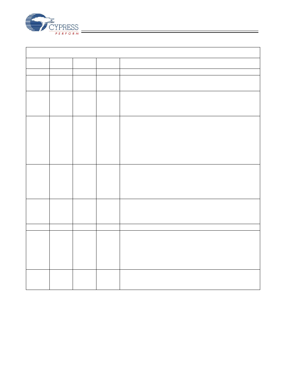
Document History Page
Document Title: CY7C1360C/CY7C1362C 9-Mbit (256K x 36/512K x 18) Pipelined SRAM
Document Number: 38-05540
REV.
ECN NO.
Issue Date
Orig. of
Change
Description of Change
**
241690
See ECN
RKF
New data sheet
*A
278130
See ECN
RKF
Changed Boundary Scan order to match the B rev of these devices
Changed TQFP pkg to Lead-free TQFP in Ordering Information section
Added comment of Lead-free BG and BZ packages availability
*B
248929
See ECN
VBL
Changed ISB1 and ISB3 from DC Characteristics table as follows:
ISB1: 225 MHz -> 130 mA, 200 MHz -> 120 mA, 167 MHz -> 110 mA
ISB3: 225 MHz -> 120 mA, 200 MHz -> 110 mA, 167 MHz -> 100 mA
Changed IDDZZ to 50 mA
Added BG and BZ pkg lead-free part numbers to ordering info section
*C
323636
See ECN
PCI
Changed frequency of 225 MHz into 250 MHz
Added t
CYC
of 4.0 ns for 250 MHz
Changed
Θ
JA
and
Θ
JC
for TQFP Package
from 25 and 9
°C/W to 29.41 and
6.13
°C/W respectively
Changed
Θ
JA
and
Θ
JC
for BGA Package
from 25 and 6
°C/W to 34.1 and
14.0
°C/W respectively
Changed
Θ
JA
and
Θ
JC
for FBGA Package
from 27 and 6
°C/W to 16.8 and
3.0
°C/W respectively
Modified address expansion as per JEDEC Standard
Removed comment of Lead-free BG and BZ packages availability
*D
332879
See ECN
PCI
Unshaded 200 and 166 MHz speed bins in the AC/DC Table and Selection
Guide
Added Address Expansion pins in the Pin Definition Table
Changed Device Width (23:18) for 119-BGA from 000000 to 101000
Added separate row for 165 -FBGA Device Width (23:18)
Modified V
OL
, V
OH
test conditions
Updated Ordering Information Table
*E
357258
See ECN
PCI
Changed from Preliminary to Final
Removed Shading on 250MHz Speed Bin in Selection Guide and AC/DC
Table
Changed I
SB2
from 30 to 40 mA
Updated Ordering Information Table
*F
377095
See ECN
PCI
Modified test condition in note# 16 from V
DDQ
< V
DD
to
V
DDQ
≤ V
DD
*G
408298
See ECN
RXU
Changed address of Cypress Semiconductor Corporation on Page# 1 from
“3901 North First Street” to “198 Champion Court”
Changed three
-
state to tri-state on page# 9 & page# 10
Modified “Input Load” to “Input Leakage Current except ZZ and MODE” in
the Electrical Characteristics Table
Replaced Package Name column with Package Diagram in the Ordering
Information table
Updated Ordering Information Table
*H
501793
See ECN
VKN
Added the Maximum Rating for Supply Voltage on V
DDQ
Relative to GND
Changed t
TH
, t
TL
from 25 ns to 20 ns and t
TDOV
from 5 ns to 10 ns in TAP
AC Switching Characteristics table.
Updated the Ordering Information table.