Depth expansion, Programmable impedance, Echo clocks – Cypress CY7C1420AV18 User Manual
Page 9: Application example
CY7C1416AV18, CY7C1427AV18
CY7C1418AV18, CY7C1420AV18
Document Number: 38-05616 Rev. *F
Page 9 of 31
Depth Expansion
Depth expansion requires replicating the LD control signal for
each bank. All other control signals can be common between
banks as appropriate.
Programmable Impedance
An external resistor, RQ, must be connected between the ZQ pin
on the SRAM and V
SS
to allow the SRAM to adjust its output
driver impedance. The value of RQ must be 5x the value of the
intended line impedance driven by the SRAM, The allowable
range of RQ to guarantee impedance matching with a tolerance
of ± 15% is between 175
Ω and 350Ω
,
with V
DDQ
= 1.5V. The
output impedance is adjusted every 1024 cycles upon power up
to account for drifts in supply voltage and temperature.
Echo Clocks
Echo clocks are provided on the DDR-II to simplify data capture
on high-speed systems. Two echo clocks are generated by the
DDR-II. CQ is referenced with respect to C and CQ is referenced
with respect to C. These are free-running clocks and are
synchronized to the output clock of the DDR-II. In the single clock
mode, CQ is generated with respect to K, and CQ is generated
with respect to K. The timings for the echo clocks is shown in the
AC Timing Table.
DLL
These chips use a Delay Lock Loop (DLL) that is designed to
function between 120 MHz and the specified maximum clock
frequency. During power up, when the DOFF is tied HIGH, the
DLL is locked after 1024 cycles of stable clock. The DLL can also
be reset by slowing or stopping the input clock K and K for a
minimum of 30 ns. However, it is not necessary to reset the DLL
to lock to the desired frequency. The DLL automatically locks
1024 clock cycles after a stable clock is presented. The DLL may
be disabled by applying ground to the DOFF pin. For information
refer to the application no
.
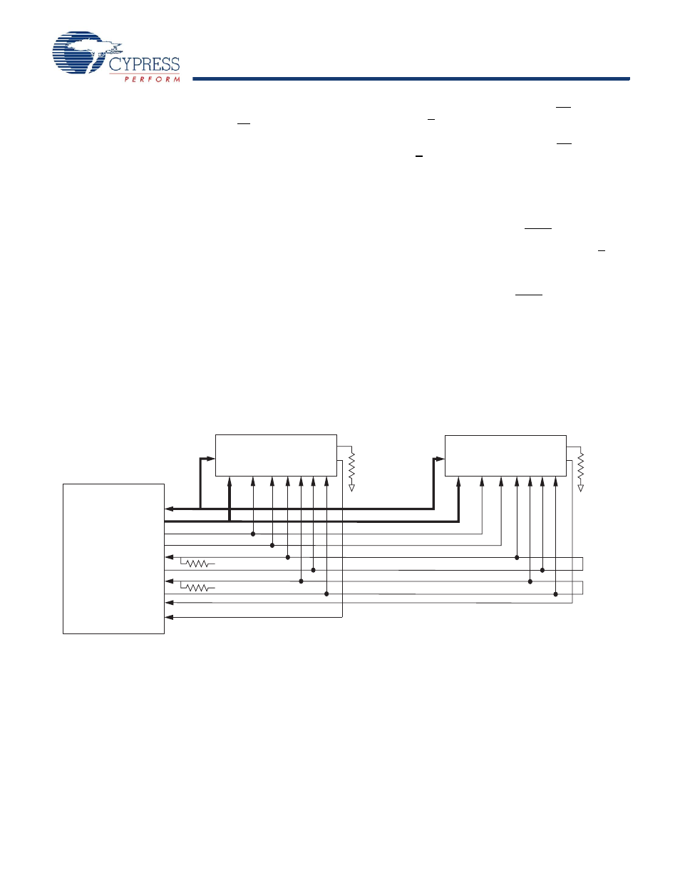
Application Example
shows two DDR-II used in an application.
Figure 1. Application Example
Vterm = 0.75V
Vterm = 0.75V
R = 50
ohms
R = 250
ohms
LD#
C C#
R/W#
DQ
A
K
LD#
C C#
R/W#
DQ
A
K
SRAM#1
SRAM#2
R
= 250ohms
BUS
MASTER
(CPU
or
ASIC)
DQ
Addresses
Cycle Start#
R/W#
Return CLK
Source CLK
Return CLK#
Source CLK#
Echo Clock1/Echo Clock#1
Echo Clock2/Echo Clock#2
ZQ
CQ/CQ#
K#
ZQ
CQ/CQ#
K#