1771-dcm switch settings, Supervisory processor logic – Rockwell Automation 1771-DCM USER MANUAL 1771-DCM User Manual
Page 24
Programming the 1771-DCM
Chapter 6
6Ć3
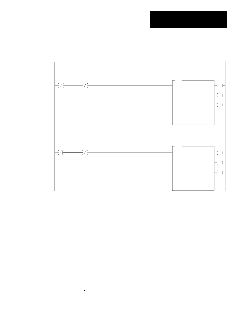
Figure 6.2
Local Processor Programming Example (PLC-5)
BTR
ENABLE BIT
Rung 2:0
PLC5 local write rung. The DCM is located in the same I/O chassis as the PLC5, and is set for block transfer. The local procesĆ
sor's write length must match the supervisory processor's read length.
N12:0
15
N12:5
15
BTW
ENABLE BIT
BTR
ENABLE BIT
N12:0
15
N12:5
15
BTW
ENABLE BIT
Rung 2:1
PLC5 local read rung. The DCM is located in the same I/O chassis as the PLC5, and is set for block transfer. The local procesĆ
sor's read length must match the supervisory processor's write length.
EN
BTW
BLOCK TRNSFR WRITE
Rack
Group
Module
Control Block
0
3
1
N12:5
DN
Data file
Length
Continuous
N13:30
17
N
ER
EN
BTR
BLOCK TRNSFR READ
Rack
Group
Module
Control Block
0
3
1
N12:0
DN
Data file
Length
Continuous
N13:30
21
N
ER
Select module operating conditions by setting switches on the module for
discrete data transfer or block transfer as follows:
Discrete Data Transfer
Block Transfer
•
Transfer Method
•
Transfer Method
•
Rack Size
•
Data Protect (If Applicable)
Set other switches as required by your application.
The addresses that you use for the 1771–DCM in the supervisory
processor’s ladder program are the addresses (RGS) to which you
configure your 1771–DCM using Switch Banks 0 and 1:
I/O Rack Number (Switch Bank 1, Switches 1 through 6).
1771-DCM Switch Settings
Supervisory Processor Logic