Anritsu MP1763C User Manual
Page 21
1-5
1.2 Specifications
1/8 output
8 data outputs, 1 clock output
300 ps or less (20-80 %)
100 ps or less (p-p)
Waveform distortion
15 % or less
Skew
150 ps or less (relative to falling edge of 1/8 clock)
Output bit rate
1/8 of fundamental frequency
50
Ω
SMA
Alternate pattern
A/B switching
input
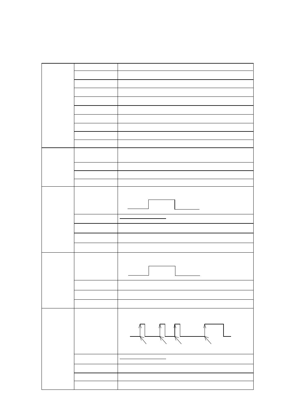
ALTN patterns A/B switching controlled by external signal
Input level
50
Ω
SMA
Output level
Error injection
input
Error inserted at rising edge by external signal
Input level
0/–1 V
50
Ω
SMA
Error
Error
Error
Error
Number of output
Output level
Rise / fall time
Pattern jitter
Load impedance
Connector
A
B
A
Input impedance
Connector
A
B
A
Output impedance
Connector
50
Ω
SMA
ECL (H: –0.9
0.2 V, L: –1.75
0.2 V)
ECL (H: –0.9
0.25 V, L: –1.75
0.25 V)
ALTN patterns A/B switching signal output
ECL (H: –0.9
0.2 V, L: –1.75
0.2 V)
Input impedance
Connector
Fundamental frequency
Minimum pulse width
1
Data length
Fundamental frequency
Minimum pulse width
1
x 128
Alternate pattern
A/B switching
output
Connector
50
Ω
Load impedance
Output level
V : 0
±200 mV Amplitude: 1 Vp-p±20 %
SMA
OH
Switching of 1/64 CLOCK, Fixed position pattern sync, and Variable
position pattern sync
Sync. output
Data polarity
Same as 1/1 DATA