Cs8130 – Cirrus Logic CS8130 User Manual
Page 2
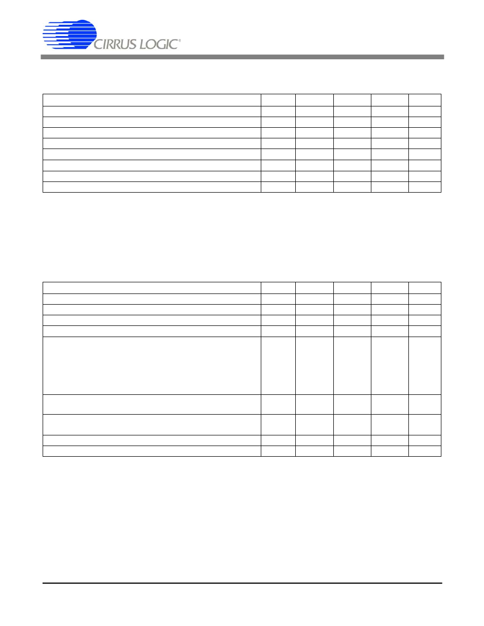
TRANSMITTER DRIVER CHARACTERISTICS (T
A
= 25
°
C; All V+ = 3.0V, Digital Input Levels: Logic 0 = 0V,
Logic 1 = V+; unless otherwise specified)
Parameter
Symbol
Min
Typ
Max
Units
Output capacitance
(Note 1)
10
TBD
pF
Output rise time (10% to 90%)
tr
-
20
50
ns
Output fall time (90% to 10%)
tf
-
20
50
ns
Overshoot over final current
-
-
25
%
On resistance
-
-
0.5
Ω
Off leakage current
-
-
20
µ
A
Output current (each driver)
(Note 2)
-
-
250
mA
Output jitter relative a jitter free input clock
-
-
200
ns
Notes:
1. Typical LED junction capacitance is 20pF.
2. 50% duty cycle, max pulse width 165
µ
s (3/16 of (1/1200 bps + 5%)).
Specifications are subject to change without notice.
RECEIVER CHARACTERISTICS (T
A
= 25
°
C; All V+ = 3.0V, Digital Input Levels: Logic 0 = 0V, Logic 1 = V+;
unless otherwise specified)
Parameter
Symbol
Min
Typ
Max
Units
Input capacitance
(Note 3)
-
10
TBD
pF
Input noise current
-
-
11
pA/rtHz
Maximum signal input current from detector
-
-
2
mA
Maximum DC input current (typically sunlight)
-
-
200
µ
A
Input current detection thresholds
RS4-0=00000:
(Programmable with a 5 bit value)
RS4-0=00001:
(Min, Max = Typical
±
30%)
RS4-0=00010:
(Note 4)
↓
RS4-0=11110:
RS4-0=11111:
-
-
16.4
↓
169.5
175
7.8
15.6
23.4
↓
242.2
250
-
-
30.4
↓
314.9
325
nA
nA
nA
"
nA
nA
Bandpass filter response
High Pass -3dB:
Low Pass -3dB:
-
-
35
700
-
-
kHz
kHz
Receiver power up time
With high (200
µ
A) dc ambient
With normal (2
µ
A) dc ambient
-
-
5
0.3
10
1
ms
ms
Turn-around time, with receiver on continuously
(Note 5)
-
5
10
ms
EMI rejection of system (0.5MHz to 100MHz).
(Note 6)
3
-
-
V/m
Notes:
3. Typical PIN diode junction capacitance is 50pF.
4. The
±
30% tolerance covers chip-to-chip variation. The temperature coefficient of the receiver
threshold setting is low. Current detection thresholds are above the DC ambient condition.
Settings of RS4-0 of less than 00010 are not practical because of noise.
5. Turn-around time is the time taken for the PIN diode receiver to recover from the IR energy
from the transmitter. The remote end of the link must wait for this time after receiving data
before transmitting a reply. This time may be reduced to <1 ms by good IR shielding from
the transmit LED to the PIN diode.
6. This is a system specification. A metal shield over the PIN diode and CS8130 is
recommended to ensure system compliance.
CS8130
2
DS134PP2
CS8130
2
DS134F1