Cs8130 – Cirrus Logic CS8130 User Manual
Page 12
Reset
Bringing the RESET pin low will force the inter-
nal logic, including the control registers, into a
known state, provided the PWRDN pin is high.
RESET is disabled if the PWRDN pin is low.
The reset state is given in each register definition
table. RESET must be low for >25 ms if using
the crystal oscillator (see Clock Generation
above).
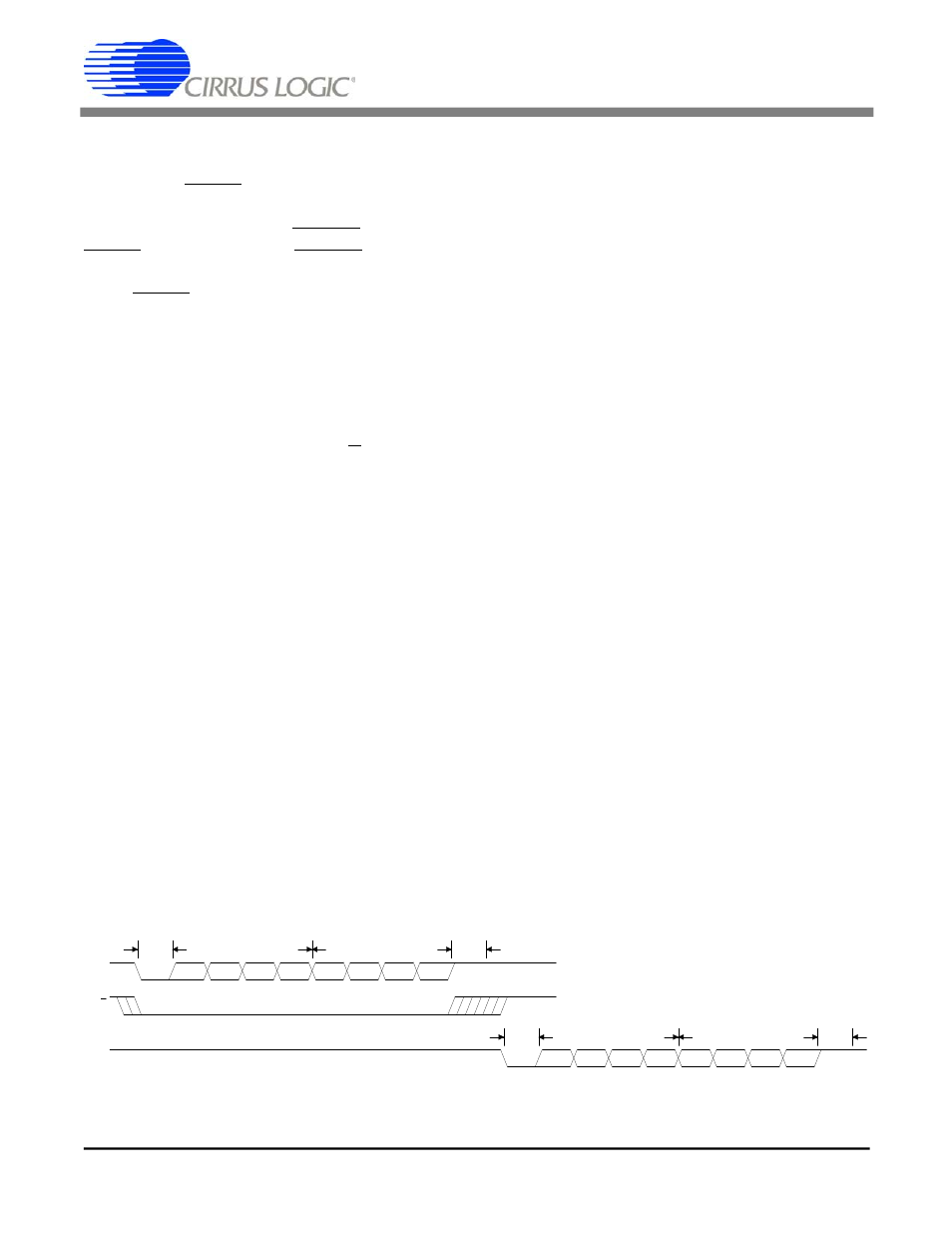
Control Register Definitions
The various control registers within the CS8130
may be written by setting the D/C pin to low,
and sending characters from the UART to the
TXD pin. The characters are interpreted as a 4-
bit address field and a 4-bit data field, as shown
in Figure 7. After the control character is re-
ceived and written into the control register, it is
optionally echoed back out the RXD pin. The
baud rate used for this control mode is whatever
is currently set in the baud rate register. If the
"load baud rate" bit is written to, then the new
baud rate takes effect after the character has been
echoed back, if echo is enabled. Otherwise, the
new baud rate is effective immediately.
One of the control registers contains a shadow
register set enable bit, which effectively becomes
the MSB of the 5-bit register address. Hence
there are 31 4-bit registers. The shadow bit must
be written to a 1 to allow access to the registers
with addresses 16 through 31. The shadow bit
register is always accessible, independent of the
state of the shadow bit. The shadow bit must be
written to 0 to enable access to registers 0
through 15.
The following tables define the detailed function
of all the registers inside the CS8130.
CD0
CD1
CD2
CD3
AD0
AD1
AD2
AD3
CD0
CD1
CD2
CD3
AD0
AD1
AD2
AD3
Start
Bit
Data
Address
Stop
Bit
Start
Bit
Data
Address
Stop
Bit
TXD
D/C
RXD
Figure 7. Control Mode Timing
CS8130
12
DS134PP2
CS8130
12
DS134F1